
Product Description
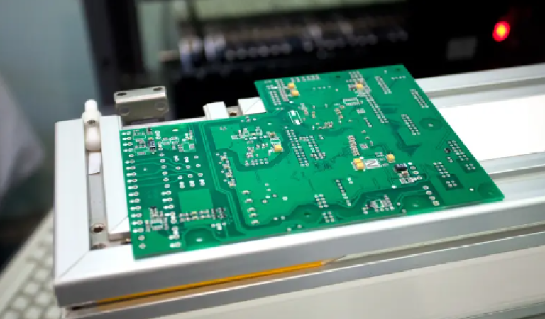
Multilayer PCBs are used when a two-layer board does not provide enough routing space, power distribution, or signal control. Extra layers can support dedicated signal paths, power planes, ground planes, and thermal copper areas.
They are often used in projects with fine-pitch components, high-speed signals, multiple power rails, compact board sizes, or higher routing density. The right layer structure should be selected from the actual electrical and mechanical requirements, not only from the component count.
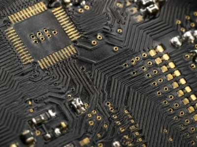
Dense Routing Around Fine-Pitch Components
More layers can create additional routing channels under BGA packages and other dense component areas. This can help avoid unnecessary trace congestion on the outer layers.
Signal and Power Plane Requirements
Internal ground and power planes can support cleaner return paths and more stable power distribution. This becomes more important when the design includes high-speed digital signals or several power domains.
Compact Board Size Requirements
A multilayer structure can support more circuitry in a limited board area. The stack-up and via design should still be reviewed to make sure the routing remains practical for manufacturing.
What We Review Before Manufacturing
A multilayer PCB project should be reviewed as a complete build package. The visible copper layout is important, but the internal structure also affects fabrication, signal behavior, drilling, lamination, and inspection planning.
Clear files help avoid repeated questions during quotation and production preparation. They also give the engineering team a better basis for checking potential DFM risks.
| Review Area | What Should Be Confirmed |
|---|---|
| Gerber files | Complete copper, solder mask, silkscreen, and board outline data |
| Drill files | Hole types, finished hole notes, and via requirements |
| Stack-up | Signal layers, power planes, ground planes, and dielectric structure |
| Material notes | Electrical, thermal, and application requirements |
| Impedance notes | Critical signals and target requirements |
| Fabrication drawing | Special instructions and acceptance requirements |
Gerber Files and Drill Data
Gerber files should include complete layer data rather than only top and bottom copper. Drill data should clearly identify finished holes, via structures, slots, and any special fabrication notes.
Stack-Up Information
For complex multilayer boards, Gerber files alone may not define the full internal dielectric structure. Stack-up notes should be included or reviewed before production, especially when impedance or high-speed signal control is required.
DFM and Engineering Review
A DFM review can help identify unclear notes, routing limitations, copper balance concerns, and assembly risks before the board enters production planning. For Gerber review, fabrication notes, and stack-up preparation, use PCB design as the related internal link.
Stack-Up Planning for Signal Control
Stack-up planning affects how signal layers, power planes, ground planes, copper thickness, and dielectric materials work together. A clear layer arrangement helps support signal return paths, routing control, and stable interlayer connections.
For high-speed or sensitive signal sections, the stack-up should be reviewed together with impedance requirements. Trace width, spacing, reference planes, dielectric thickness, and material selection all affect the final result.
Signal Layer Placement
Critical signal layers should have suitable reference planes. This helps reduce unwanted coupling and supports more stable signal behavior.
Ground Plane Continuity
Ground plane interruptions can affect return paths and increase noise risk. High-speed routing should be checked together with the plane structure below or above the trace.
Controlled Impedance Requirements
Controlled impedance should not be treated as a simple note in the fabrication files. The target requirements must match the final stack-up, trace geometry, copper thickness, and material construction.
For impedance planning and signal integrity support, use Impedance Controlled PCBs as the relevant internal link.
Material Selection for Multilayer PCB Projects
Material selection should match the electrical, thermal, and mechanical needs of the application. A standard laminate may suit many general electronics projects, while other designs may require further review for heat resistance, high-frequency signals, or demanding assembly conditions.
The material decision should be based on the actual project requirements. It should not be made only by material name, brand name, or cost.
Thermal Reliability Requirements
Projects with higher thermal stress may need additional material review. This can include applications with power devices, processors, RF modules, or repeated thermal cycling.
For high-temperature application requirements, use High Tg PCB as the supporting internal link.
High-Frequency and RF Requirements
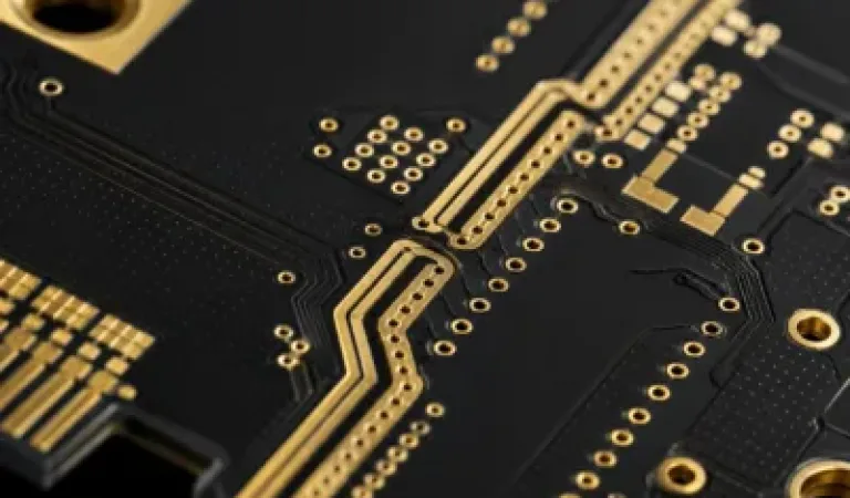
Communication, RF, and high-speed designs may require closer review of dielectric behavior and signal loss. The material, stack-up, copper surface, and routing geometry should be considered together.
For RF, low-loss material, and high-frequency routing projects, use High Frequency PCB as the related internal link.
Via Design and Dense Routing
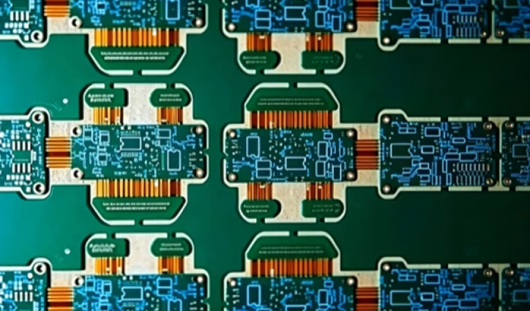
Via design connects the copper layers inside a multilayer PCB. Standard through-hole vias work well for many projects. More complex routing may require blind vias, buried vias, or HDI structures.
The correct via structure depends on routing density, component pitch, layer arrangement, electrical needs, and production requirements. Adding more complex vias without reviewing the signal path or manufacturing impact can create unnecessary risk.
Fine-Pitch Routing and BGA Escape Areas
Fine-pitch packages can require more routing space and smaller transition areas. The design should be reviewed to confirm whether a standard multilayer structure is sufficient.
HDI Structure Requirements
Projects with microvias, fine lines, stacked vias, or more complex layer transitions may need an HDI approach. In these cases, use HDI PCBs as the supporting internal link.
Copper Balance and Thermal Planning
Copper balance affects lamination stability, plating consistency, board flatness, and heat distribution. Large differences in copper coverage between layers should be identified during the engineering review.
Thermal planning is also important for boards with high-current paths, power devices, processors, or dense copper areas. Copper planes, thermal pads, via arrays, and material selection can affect heat transfer through the finished board.
Uneven Copper Distribution
Large copper-filled regions on one layer and sparse routing on another may affect manufacturing balance. These areas should be visible in the Gerber files and reviewed before fabrication.
High-Current and Thermal Paths
Projects with stronger power distribution requirements may need additional copper and thermal planning. For high-current paths and heavier copper requirements, use Heavy Copper PCBs as the related internal link.
Assembly and Testing Considerations
Bare PCB fabrication and assembly planning should be connected early. A board may be electrically correct but still create assembly problems if component spacing, pad design, solder mask openings, or test access are not practical.
For PCBA projects, the BOM, pick-and-place file, assembly drawing, polarity notes, and test requirements should be reviewed together with the bare board files.
| Assembly Area | Files or Information to Prepare |
| BOM review | Manufacturer part numbers and approved alternatives |
| Component placement | Pick-and-place file and placement data |
| Assembly drawing | Polarity, connector, and special assembly notes |
| BGA or QFN packages | Inspection requirement where needed |
| Testing plan | Test points, functional checks, and acceptance criteria |
BOM and Assembly File Review
A complete BOM helps identify component sourcing questions before assembly planning. Assembly drawings and placement files help clarify polarity, connector orientation, and special process requirements.
For BOM review, SMT preparation, and test planning, use PCBA processing as the main internal link.
BGA and Hidden Solder Joint Inspection
Projects with BGA packages may need inspection planning for hidden solder joints. The inspection method should be confirmed from the component package, board layout, and project requirement.
For BGA-related assembly support, use BGA Assembly as the related internal link.
Files Required for Quotation
A multilayer PCB quotation should be based on a complete project package. The internal layer structure can affect material, lamination, drilling, impedance, and assembly planning, so an image or board outline alone is not enough.
Please provide the following information where available:
Preparing Your Multilayer PCB Project
Multilayer PCB manufacturing should begin with a clear review of the stack-up, material notes, via structure, copper balance, impedance requirements, and assembly needs.
Before production planning, make sure the Gerber files, drill data, fabrication notes, and assembly documents reflect the final design intent. This helps reduce avoidable engineering questions and manufacturing risk.
To request a quotation, please send your Gerber files, BOM, assembly drawings, stack-up notes, and quantity requirements to sales@toplinecircuit.com.