


With the rapid development of 5G communication, millimeter-wave radar, satellite communication, RF modules, and high-speed wireless devices, high-frequency PCBs have become a critical foundation for modern RF and microwave systems. Compared with conventional PCBs, high-frequency applications require better signal integrity, more stable impedance control, and lower transmission loss. In high-frequency environments, insufficient material performance or poor manufacturing precision can easily cause signal attenuation, unstable transmission, and electromagnetic interference, directly affecting overall system performance. Double-sided RF ENIG high-frequency PCBs are specifically designed for RF and microwave applications. By combining ENIG surface treatment with Taconic TSM-DS3 high-frequency materials, these PCBs provide excellent conductivity, lower signal loss, and long-term operational stability, making them highly important in modern high-speed communication systems.
What Is a Double-Sided RF ENIG High-Frequency PCB?
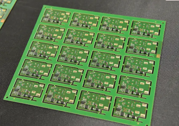
A double-sided RF ENIG high-frequency PCB is a dual-layer printed circuit board specifically designed for high-frequency wireless communication and microwave systems.
Main product features include:
- Double-sided high-frequency circuit structure.
- ENIG (Electroless Nickel Immersion Gold) surface finish.
- Taconic TSM-DS3 high-frequency material.
- Lower dielectric loss.
- More stable impedance control capability.
- Higher electrical conductivity.
- Better corrosion resistance.
- More reliable soldering performance.
Compared with standard FR4 PCBs, high-frequency PCBs are better suited for GHz-level and millimeter-wave applications.
Why Is Taconic TSM-DS3 Suitable for High-Frequency Applications?
In RF and microwave systems, PCB materials directly affect high-speed signal transmission quality.
Taconic TSM-DS3 is a high-performance high-frequency material with the following advantages:
| Material Property | Taconic TSM-DS3 Advantage | Impact on High-Frequency Systems |
| Low Dielectric Constant | More stable high-frequency transmission | Reduces signal delay |
| Low Loss Factor | Reduces high-frequency signal attenuation | Improves transmission efficiency |
| High-Frequency Stability | Supports GHz-level applications | Enhances system stability |
| Thermal Stability | Stable performance under high temperatures | Improves reliability |
| Low Moisture Absorption | Better environmental adaptability | Reduces performance fluctuation |
| Impedance Consistency | More accurate impedance control | Improves signal integrity |
For millimeter-wave communication and RF modules, material stability directly influences communication quality and overall system performance.
Why Is ENIG Surface Finish Ideal for RF High-Frequency PCBs?
ENIG (Electroless Nickel Immersion Gold) is one of the most common surface finishes used in high-frequency PCBs.
Compared with traditional HASL finishes, ENIG provides several important advantages:
- Better surface flatness.
- More suitable for high-frequency circuits.
- More stable electrical conductivity.
- Stronger corrosion resistance.
- Improved soldering reliability.
- Longer storage life.
- Better compatibility with precision assembly.
In high-frequency RF systems, surface roughness directly affects signal loss, while ENIG surface treatment helps reduce transmission loss during high-frequency operation.
Why Are Double-Sided High-Frequency PCBs Suitable for RF and Microwave Systems?
Although double-sided high-frequency PCBs have relatively simple structures, they still offer major advantages in many RF modules and microwave devices.
Double-sided structures provide:
- Shorter signal transmission paths.
- Lower high-frequency loss.
- More stable impedance control.
- Lower manufacturing cost.
- Higher processing efficiency.
- Better suitability for compact RF modules.
Double-sided high-frequency PCBs remain widely used in wireless antennas, power amplifiers, and RF filter modules.
What Are the Key Manufacturing Requirements for Double-Sided RF High-Frequency PCBs?
High-frequency PCBs require much higher manufacturing precision than standard PCBs.
Key production controls include:
- Stability of high-frequency material lamination.
- Precision of high-frequency trace dimensions.
- Copper surface roughness control.
- High-frequency impedance consistency.
- ENIG thickness control.
- Optimization of high-frequency signal return paths.
- Drilling precision control.
- High-frequency trace etching accuracy.
In GHz-level systems, even very small trace deviations may affect overall system performance.
Manufacturing high-frequency PCBs requires not only advanced equipment but also extensive RF engineering experience.
Main Applications of Double-Sided RF ENIG High-Frequency PCBs
As wireless communication technology continues to advance rapidly, high-frequency PCBs are now widely used in many high-end industries.
- 5G RF Communication Modules: Support stable high-speed wireless signal transmission.
- Microwave Communication Equipment: Suitable for high-frequency long-distance communication systems.
- Millimeter-Wave Radar Systems: Improve high-speed detection and data processing capability.
- Satellite Communication Modules: Meet the requirements for low-loss high-frequency transmission.
- Wireless Antenna Systems: Enhance signal transmission and reception stability.
- RF Power Amplifiers: Improve high-frequency operational efficiency and stability.
Why Is Low-Loss Design Becoming Increasingly Important in High-Frequency PCBs?
In high-frequency communication systems, signal loss directly affects communication distance and transmission stability.
Excessive PCB loss may cause:
- High-frequency signal attenuation.
- Reduced data transmission speed.
- Lower communication stability.
- Increased heat generation.
- Reduced system efficiency.
Low-loss high-frequency PCBs help to:
- Improve high-speed signal integrity.
- Reduce transmission loss.
- Enhance system stability.
- Improve wireless communication quality.
- Extend equipment service life.
As millimeter-wave and high-speed wireless technologies continue to evolve, low-loss design has become one of the most important directions in high-frequency PCB development.
Why Choose Our Double-Sided RF ENIG High-Frequency PCB Products?
RF and microwave systems require extremely high levels of PCB stability, consistency, and high-frequency performance.
Our high-frequency PCB products provide the following advantages:
- Taconic TSM-DS3 high-frequency materials.
- Support for GHz-level applications.
- Low dielectric and low-loss design.
- High-precision impedance control capability.
- ENIG surface finish for improved conductivity and solderability.
- Extensive high-frequency PCB manufacturing experience.
- Support for rapid prototyping and mass production.
- Strict quality inspection processes.
- Stable performance in complex environments.
We provide reliable PCB manufacturing support for 5G communication, RF modules, millimeter-wave systems, and advanced wireless devices.
As 5G, millimeter-wave communication, and high-speed wireless technologies continue to advance, the demand for low-loss, high-stability, and highly reliable high-frequency PCBs is increasing rapidly. Double-sided RF ENIG high-frequency PCBs have become an important foundation in modern RF and microwave systems thanks to their excellent conductivity, stable impedance control, and strong environmental adaptability. Topline Circuit specializes in high-frequency PCBs, HDI PCBs, and complex multilayer PCB manufacturing, providing reliable PCB solutions for RF communication, millimeter-wave modules, satellite communication, and advanced wireless systems. For more information about customized high-frequency PCB solutions, feel free to contact us.
Email: sales@toplinecircuit.com
VK: vk.com/id1058761391
WhatsApp / WeChat: +86 134 2515 6463
Address: 3/F, Building B3, Yanchuan North Industrial Park, Yanluo Street, Bao’an District, Shenzhen, China


")

