


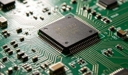
The stable operation of RF modules relies on precise impedance control; impedance deviation can lead to signal loss and unstable communication. Our customization service is specifically designed for various types of RF modules, compatible with the full frequency range, balancing performance, reliability and cost to help devices achieve better RF performance.
Core Advantages
Combined with the core operational needs of RF modules, our impedance-controlled PCB customization forms core competitiveness in terms of precision, material selection, craftsmanship and other aspects. The specific advantages are as follows:
- High impedance precision, with deviation controlled within ±1%~±5%, compatible with standard impedances such as 50Ω, 75Ω and 100Ω, ensuring stable high-frequency signal transmission.
- Flexible material selection, available in Rogers, PI, modified low-loss FR-4 and other substrates, adapting to different frequency bands and working environment requirements.
- Precise craftsmanship, adopting LDI, vacuum lamination and other processes, with small deviations in line width and dielectric thickness, and high consistency in mass production.
- Strong customization, flexible design according to module size, pin layout, etc., without the need for customers to adjust module design.
- Full-process quality control, with a mass production qualification rate of over 99.5%, reducing customers’ assembly and commissioning costs.
The above core advantages support each other, not only ensuring the stable operation of RF modules, but also effectively reducing customers’ R&D and production costs.
Main Features
| Feature Category | Detailed Description |
| Full Frequency Range Compatibility | Covers 1GHz to millimeter wave, meeting the needs of multiple scenarios such as WiFi 7, 5G and automotive radar |
| Design Guarantee | Combination of simulation and actual measurement, avoiding design deviations in advance, shortening customization cycle and reducing trial-and-error costs |
| Anti-interference Capability | Integrated anti-interference design, optimized grounding and shielding structure, adapting to complex interference environments |
| Cost-performance Balance | High-frequency substrates are used for core links, and costs are controlled in non-critical areas, balancing performance and cost-effectiveness |
| Customization Service | One-stop service, supporting small-batch trial production (minimum 10 pieces), with samples delivered as fast as 3 days |
Frequently Asked Questions
Q1: Why can’t ordinary PCBs be used instead of impedance-controlled PCBs for RF modules?
A1: Ordinary PCBs have large impedance deviations (10%-20%), which can cause signal reflection and loss, affecting module communication. In high-frequency scenarios, a deviation of 1Ω may cause the device to fail to operate normally.
Q2: How to determine the required impedance value during customization?
A2: It is determined by the module chip interface and signal rate, with common values of 50Ω, 100Ω and 75Ω. Customers provide relevant parameters, and our engineers accurately determine and optimize them.
Q3: How to ensure the consistency of impedance precision in mass customization?
A3: Full-process quality control is adopted, with strict inspection of substrates and each production link, and 100% testing of finished products to control mass deviation within the agreed range.
Q4: Are there differences in PCB customization for RF modules in different working environments?
A4: Yes, the differences mainly lie in substrate and process selection. For example, automotive modules require temperature resistance and vibration resistance, while consumer modules can use low-cost substrates.
Application Scenarios
Our impedance-controlled PCB customization for RF modules is suitable for various fields and types of RF equipment, covering different frequency bands and working environments. The specific application scenarios are as follows:
- Ion RF modules: Bluetooth, WiFi, etc., suitable for smart home and wearable devices, focusing on miniaturization and low cost.
- 5G communication equipment: Base stations, CPE terminals, with high signal rate, requiring high-precision impedance and low-loss substrates.
- Automotive electronics: Millimeter wave radar, etc., requiring temperature resistance, vibration resistance and high-precision impedance.
- Satellite communication: Resistant to extreme environments, using low-loss and high-precision substrates.
- Medical equipment: High reliability and low interference, complying with industry standards.
Test instruments: Extremely high impedance precision to ensure accurate test data.
In any scenario, we can customize adaptive solutions according to specific needs to help various RF devices exert optimal performance.


")

