


As electronic products continue to develop toward thinner, smaller, and more reliable designs, custom 4-layer rigid-flex PCBs have become an important choice for many mid-to-high-end electronic devices. By combining the stable support capability of rigid circuit boards with the bendable and space-crossing connection capability of flexible circuit boards, rigid-flex PCBs not only reduce the use of connectors and flat cables, but also make internal product structures more compact, routing more flexible, and assembly more stable.
For power equipment, medical devices, automotive components, and industrial control equipment, 4-layer rigid-flex PCBs are often not an “optional solution,” but a more practical solution for complex structures and high-reliability applications.When many customers first learn about this type of product, the first concern is usually not the layer count, but what problems it can actually solve. In fact, the greatest value of a 4-layer rigid-flex PCB lies in its ability to integrate “areas requiring component installation” and “areas requiring flexible connections” into a single board. This allows circuit design to evolve from a flat layout into a three-dimensional structure while improving overall system stability.
What Is a 4-Layer Rigid-Flex PCB?
Basic Definition of a 4-Layer Rigid-Flex PCB
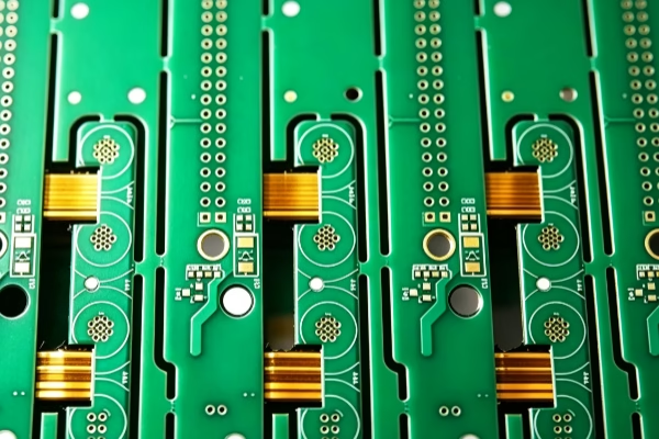
A 4-layer rigid-flex PCB is a PCB structure composed of four conductive layers while simultaneously containing rigid areas and flexible areas.Unlike ordinary rigid boards, it does not rely solely on rigid structures to complete all connections. Instead, flexible circuits are embedded into the rigid structure, allowing local areas of the product to bend, fold, or cross spaces for connections.Compared with standard FPCs, it also provides more stable rigid support, enabling higher-density component layouts and more complex system integration requirements.The essence of this structure is that the circuit board is no longer only suitable for “flat installation,” but can adapt to three-dimensional assembly environments.For example, inside space-constrained equipment, flexible areas can replace traditional wiring harnesses to connect different modules, while rigid areas are responsible for component soldering and functional support. This reduces connection points and improves overall product reliability.
Main Features and Advantages
The advantages of a 4-layer rigid-flex PCB are not simply that “it can bend,” but that “it can operate stably in complex environments.”It usually uses polyimide (PI) instead of traditional FR4 material as the substrate for the flexible area because PI offers excellent thermal stability and flexibility, enabling it to withstand high temperatures and repeated bending.The use of flexible materials makes surface mounting easier and also simplifies the implementation of complex circuit designs. Meanwhile, the 4-layer structure provides sufficient routing layers and electrical performance support within limited space.
| Feature | Description |
| Bendable connections | Flexible areas can cross different mounting planes, reducing wiring harnesses and connectors |
| More compact structure | Suitable for miniaturized and lightweight device layouts |
| Higher reliability | Reduces plug-in points and solder joints, lowering the risk of poor contact |
| Adapts to complex designs | Suitable for multi-module integration and 3D assembly environments |
| Strong high-temperature resistance | Flexible areas commonly use PI material, suitable for higher-temperature applications |
Main Application Areas
4-layer rigid-flex PCBs are commonly used in products with high requirements for structure, performance, and reliability.Because they combine the advantages of rigid boards and flexible boards, they are widely used in:
· Power equipment
· Medical devices
· Automotive components
· Industrial control equipment
· Communication modules
In these fields, circuit boards must not only complete signal transmission but also withstand space constraints, long-term vibration, high-temperature environments, and complex installation conditions. Therefore, the value of rigid-flex structures is very significant.
| Application Field | Typical Application | Design Value |
| Medical devices | Detection modules, control boards | High reliability and stability |
| Automotive components | Vehicle control systems, sensor modules | Vibration resistance and environmental durability |
| Industrial control | Automation equipment, control terminals | Strong spatial adaptability |
| Power equipment | Monitoring and control systems | Compact structure and stable operation |
| Communication equipment | Module interconnection, signal transmission | Easier high-speed connection and layout |
How Are 4-Layer Rigid-Flex PCBs Manufactured?
Requirement Confirmation and Structural Planning
Before starting the design, the application environment, operating temperature, bending method, space limitations, and signal requirements must first be clarified..The biggest difference between a 4-layer rigid-flex PCB and a standard PCB is that it must balance both electrical performance and mechanical performance, making early-stage planning extremely important.
Engineers usually first divide the rigid areas and flexible areas, determine which areas require component installation, which areas connect different modules, which positions are bending areas, and which traces belong to high-speed signal links.If planning is unclear at this stage, problems such as bending interference, crowded routing, assembly difficulties, or insufficient reliability may occur later.
Stackup Design and Electrical Planning
The core purpose of the stackup design of a 4-layer rigid-flex PCB is to create stable reference relationships among signal layers, power layers, and ground layers.A common approach is to place critical traces as close as possible to complete ground planes to reduce impedance fluctuations and signal interference.For flexible areas, stress distribution after bending must also be considered. Excessive vias, pads, or sharp corners should be avoided in bending areas whenever possible..A well-designed stackup not only improves electrical performance but also extends the lifespan of flexible areas.
Manufacturing and Lamination Process
The manufacturing process of a 4-layer rigid-flex PCB is generally more complex than that of ordinary rigid boards.
It usually includes:Inner layer fabrication、AOI inspection、Lamination、Drilling、Hole metallization、Outer layer imaging、Surface treatment、Profile machining、Electrical testing.
Because rigid materials and flexible materials have different physical properties, temperature, pressure, and alignment accuracy must be strictly controlled during lamination. Otherwise, problems such as delamination, bubbles, warping, or layer misalignment may occur.
For higher-requirement projects, manufacturability evaluations are also conducted before production to ensure the design can smoothly enter mass production.
How to Improve the Quality of 4-Layer Rigid-Flex PCBs
Signal Integrity and Impedance Control
In 4-layer rigid-flex PCB design, impedance control is a very important factor.Once high-speed signals encounter impedance discontinuities, problems such as reflection, crosstalk, and timing deviation may occur, thereby affecting overall system performance.To ensure signal integrity, engineers usually precisely control:
· Trace width
· Trace spacing
· Copper thickness
· Dielectric thickness
High-speed signals are also placed as close as possible to continuous reference planes.At the same time, differential signals require consistent trace length and spacing to maintain synchronization and anti-interference capability.
Flexible Area Design Details
Flexible areas are the sections most likely to encounter problems in rigid-flex PCBs, so the design must be handled more carefully.Routing in flexible areas cannot simply copy rigid-board design methods. Instead, the focus should be on:
· Bending direction
· Bending radius
· Trace stress distribution
It is important to note that:
Traces should avoid 90-degree corners to reduce stress concentration caused by sharp angles;The number of vias should be minimized because vias weaken the mechanical strength of flexible areas;If the product requires frequent bending, flexible areas usually use copper materials better suited for dynamic bending along with thinner trace designs.Only in this way can long-term stability be maintained during actual use.
Crosstalk and EMI Optimization
| Optimization Direction | Specific Method | Function |
| Ground plane integrity | Maintain continuous reference planes | Reduce noise and return path issues |
| Reasonable spacing | Leave sufficient spacing between sensitive traces | Reduce crosstalk |
| Partitioned routing | Separate analog, digital, and high-speed signals | Improve system stability |
| Reduce vias | Minimize layer switching in high-speed links | Lower parasitic parameters |
| Symmetrical layout | Maintain consistent differential pair length and spacing | Improve signal quality |
Main Specification Reference
Many customers also pay attention to specific specification parameters when customizing 4-layer rigid-flex PCBs.According to different product requirements, common specifications include:
| Item | Common Parameters |
| Component spacing/width | 4/3 MIL |
| Surface thickness | 0.2 mm |
| Board thickness range | 0.5 mm ~ 3.0 mm |
| Maximum size | 18″ × 24″ |
| Surface finish | ENIG / HASL / OSP |
Among surface treatments, ENIG is the most common because it offers good flatness and stable soldering performance. Meanwhile, HASL and OSP can also be selected according to product requirements.Different surface treatment methods affect soldering performance, oxidation resistance, and application scenarios, so selection should be based on actual assembly processes.
What Materials Are Required for Manufacturing 4-Layer Rigid-Flex PCBs?
Flexible Area Materials
Flexible areas usually use polyimide (PI) materials instead of FR4.The biggest advantage of PI materials is their excellent thermal stability and flexibility, making them suitable for high-temperature applications and bending applications.They help circuits achieve crossover connections and folding in limited spaces while maintaining good mechanical reliability.The conductor materials used in flexible areas are also important because they must balance conductivity and bending durability. Therefore, material selection places greater emphasis on ductility and fatigue life.
Rigid Area Materials
Rigid areas generally use FR4 materials because they offer:
· High mechanical strength
· Dimensional stability
· Moderate cost
· Mature manufacturing processes
These properties make FR4 suitable for supporting components and high-density soldering.If products require lower signal loss, more suitable high-speed transmission material solutions can also be selected according to actual needs.The purpose of rigid areas is not “bending,” but “stability,” so the material focus is on support capability, thermal stability, and assembly compatibility.
Common Material Combination Table
| Area | Common Material | Functional Role |
| Flexible area substrate | PI (Polyimide) | Provides bending capability and heat resistance |
| Flexible area conductor | Rolled annealed copper / high-ductility copper | Suitable for repeated bending |
| Rigid area substrate | FR4 | Provides structural support and component installation |
| Surface treatment | ENIG / HASL / OSP | Improves soldering and oxidation resistance |
| Reinforcement material | Aluminum or other stiffening structures | Improves local strength |
Frequently Asked Questions
Why Are 4-Layer Rigid-Flex PCBs Usually More Valuable Than Standard PCBs?
Many customers want to know why a 4-layer rigid-flex PCB has higher value even though both are circuit boards.The reason is straightforward: it solves the problems of “space, reliability, and structural flexibility” that ordinary PCBs cannot handle simultaneously.Although ordinary rigid boards have lower costs, they often require a large number of connectors and flat cables in complex 3D assemblies. This not only occupies space but also increases failure points.
On the other hand, purely flexible boards can bend but are not suitable for long-term support of high-density components.4-layer rigid-flex PCBs combine the advantages of both, allowing one board to simultaneously handle support, connection, transmission, and layout functions.For industries such as medical devices, automotive electronics, and industrial control systems, this integrated structure not only reduces assembly steps but also improves overall system stability and long-term reliability.Therefore, it is often not simply a “higher-cost solution,” but a higher-value solution better suited for complex products.
Why Choose Topline Circuit for Custom 4-Layer Rigid-Flex PCBs?
Founded in 2000 and headquartered in Shenzhen, China, Topline Circuit is an electronic solutions provider offering PCB layout, manufacturing, assembly, testing, and verification services.
Our products include:
· High-reliability flexible circuit boards
· Rigid-flex PCBs
· RF/microwave circuit boards
· HDI circuit boards
· Rigid circuit boards
As a recognized technology-oriented manufacturer, we provide truly fast delivery cycles, and all solutions are completed in-house—from design and manufacturing to testing—creating a more complete one-stop service experience.Our circuit boards are trusted in industries such as:Government projects、Medical equipment、Instrumentation、Aerospace、Industrial applications、Communication systems.We specialize in providing high-performance and highly reliable PCB printed circuit board solutions. Whether for consumer electronics, industrial applications, or communication equipment, we can customize the most suitable products according to your requirements.If needed, please contact us via email at [sales@toplinecircuit.com](mailto:sales@toplinecircuit.com) for quotation and consultation support.


")

