


As electronic products continue to evolve toward lightweight design, high integration, and high reliability, custom 6-layer rigid-flex PCBs have become an important solution in consumer electronics, industrial control systems, medical equipment, and communication products. Compared with traditional PCBs, 6-layer rigid-flex PCBs not only save space, but also reduce the number of connectors while improving overall stability and anti-interference capability. For products requiring complex routing, dynamic bending, and high-density installation, rigid-flex PCBs are no longer just an “upgrade option,” but have become one of the core structures in many high-end electronic devices.
A 6-layer rigid-flex PCB combines the dual advantages of rigid PCBs and flexible FPCs. It can provide stable component support while also meeting the requirements of space folding, dynamic connection, and complex installation. Especially as the internal space of modern electronic products becomes increasingly compact, traditional flat cables and connectors can no longer meet high-reliability requirements. In contrast, rigid-flex structures can reduce volume while improving overall electrical performance and assembly efficiency.
What Is a Custom 6-Layer Rigid-Flex PCB?
What Is a 6-Layer Rigid-Flex PCB?
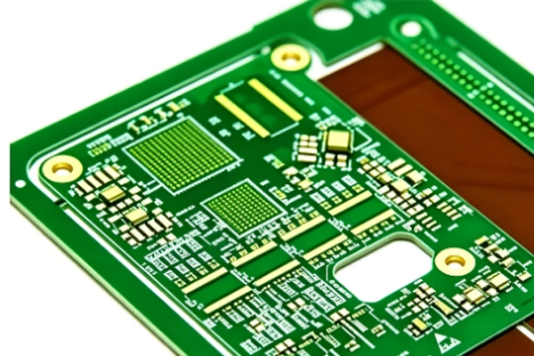
A 6-layer rigid-flex PCB is a PCB structure formed by combining 6 conductive circuit layers with flexible circuit areas and rigid circuit areas. Through a lamination process, flexible materials and rigid materials are integrated into the same circuit board, allowing the product to have both the stability of a standard PCB and the bendability of flexible circuits.
It is not simply a combination of a traditional PCB and an FPC, but a truly integrated structure. The rigid areas are usually used for mounting chips, interfaces, connectors, and other components, while the flexible areas connect different modules and enable bending, folding, or spatial crossover. This structure reduces the number of traditional cables and connectors, thereby lowering the risk of poor contact and improving overall reliability.
Why Is Custom 6-Layer Rigid-Flex PCB Needed?
As electronic devices become increasingly miniaturized, the internal space of many products can no longer accommodate traditional connection solutions. Standard PCBs are stable but cannot bend, while FPCs are flexible but have limited load-bearing capability. Therefore, 6-layer rigid-flex PCBs have become an important solution for many complex products.
Key Advantages of Custom 6-Layer Rigid-Flex PCBs:
· Save internal product space
· Reduce the number of connectors used
· Improve vibration resistance
· Enhance signal transmission stability
· Improve overall product reliability
· Enable complex three-dimensional structure installation
Especially in high-density electronic equipment, rigid-flex structures can significantly reduce routing difficulty and improve overall product integration.
Main Application Areas of 6-Layer Rigid-Flex Circuit Boards
| Application Industry | Main Application | Structural Advantage |
| Consumer electronics | Smartphones, tablets, foldable devices | Miniaturization and lightweight design |
| Medical equipment | Medical testing instruments, monitoring devices | High reliability and stable connections |
| Industrial control | Automation control modules | Vibration resistance and durability in harsh environments |
| Communication equipment | Signal modules, networking devices | Stable high-speed signal transmission |
| Aerospace | Precision electronic control systems | High reliability and lightweight structure |
| Automotive electronics | Vehicle cameras, control modules | High-temperature resistance and anti-interference capability |
How Are 6-Layer Rigid-Flex PCBs Manufactured?
Preliminary Structural Design and Functional Planning
Before formal production begins, engineers must divide the functional areas according to the product structure. Areas requiring rigid support, areas requiring flexible bending, and areas belonging to high-speed signal regions must all be planned in advance.At this stage, not only electrical performance but also actual installation space must be considered. Since rigid-flex PCBs are usually applied inside structurally complex products, both electronic performance and mechanical structure must be taken into account during design.
If the initial design is unreasonable, the following problems may occur later:
· Cracking in bending areas
· Unstable impedance
· Severe signal interference
· Difficult product assembly
Therefore, structural planning is one of the most critical steps in the entire project.
PCB Stackup Design and Routing Layout
A 6-layer rigid-flex PCB usually distributes signal layers, power layers, and ground layers reasonably.For example:
| Layer Structure | Function |
| L1 | Signal layer |
| L2 | Ground layer |
| L3 | Signal layer |
| L4 | Power layer |
| L5 | Ground layer |
| L6 | Signal layer |
This structure can effectively control impedance while reducing crosstalk and EMI issues.In flexible areas, routing design should also avoid:90-degree corners、Excessively dense vias、Overly thick copper layers、Improper bending structures..Because all these factors can affect the lifespan of flexible areas.
Lamination and Manufacturing Process
The manufacturing process of 6-layer rigid-flex PCBs is more complex than that of ordinary PCBs.The main processes include:Inner layer circuit fabrication、AOI inspection、Lamination、Drilling、Hole metallization、Outer layer circuit fabrication、Surface treatment、Profile machining、Electrical testing、Final inspection.Since flexible materials and rigid materials have different thermal expansion coefficients, the lamination process requires extremely high precision.
If temperature control is unstable, the following issues can easily occur:
· Delamination
· Air bubbles
· Warping
· Alignment deviation
Therefore, manufacturing experience has a significant impact on product quality.
How to Improve the Quality of 6-Layer Rigid-Flex PCBs?
Impedance Control and Signal Integrity
In high-speed electronic products, impedance control is extremely important. If impedance is unstable, it can easily lead to:Signal reflection、Data errors、Increased EMI、Unstable high-speed interfaces.Therefore, in 6-layer rigid-flex PCBs, high-speed signals are usually routed close to complete ground planes to form stable return paths.
For differential signals, the following must also be controlled:
· Trace width
· Trace spacing
· Copper thickness
· Dielectric thickness
Only in this way can stable signal transmission be ensured.
Crosstalk and EMI Optimization Solutions
| Technical Direction | Optimization Method | Effect |
| Ground plane integrity | Maintain continuous reference planes | Reduce noise |
| Trace spacing control | Increase spacing between sensitive traces | Reduce crosstalk |
| Differential design | Length matching | Improve signal stability |
| Reduce vias | Lower parasitic parameters | Improve high-speed performance |
| Partitioned routing | Separate analog and digital circuits | Reduce EMI |
Flexible Area Design Details
Flexible area design is a very important part of rigid-flex PCBs because it directly affects the bending lifespan, connection stability, and long-term reliability of the circuit board.Therefore, flexible areas cannot simply follow ordinary PCB routing methods. Instead, they must fully consider the impact of mechanical stress and dynamic bending.Under normal circumstances, flexible areas try to avoid 90-degree trace corners because sharp corners can easily cause stress concentration, increasing the risk of copper foil cracking. Therefore, most designs use arc routing or beveled transitions.At the same time, trace directions are usually arranged perpendicular to the bending direction as much as possible to reduce tensile stress on copper traces during bending.
In addition, the number of vias inside flexible areas is minimized whenever possible because vias reduce the mechanical strength of flexible areas and can easily cause cracks or conduction abnormalities during long-term bending.For products requiring frequent dynamic bending, rolled annealed copper materials and thinner copper layers are preferred to improve bending resistance.In addition, Coverlay film is also an important protective layer in flexible areas. It not only improves insulation performance but also effectively protects circuits from external friction and humid environments.Flexible area design is not simply about “allowing circuits to bend,” but more importantly about ensuring stable electrical performance and structural reliability during long-term product use.
What Materials Are Required for Manufacturing 6-Layer Rigid-Flex PCBs?
When manufacturing 6-layer rigid-flex PCBs, materials are generally divided into flexible area materials and rigid area materials.
Flexible Area Material Selection:
PI (polyimide) substrates are generally used because PI provides excellent high-temperature resistance, flexibility, and bending durability, meeting the repeated bending and complex installation requirements of rigid-flex PCBs.Flexible conductors usually use rolled annealed copper. Compared with ordinary electrolytic copper, rolled copper has better ductility and is more suitable for dynamic bending environments.In addition, flexible areas are also combined with Coverlay films to protect circuits and improve insulation performance.
Rigid Area Material Selection:
FR-4 substrates are used because they provide high mechanical strength, dimensional stability, and mature manufacturing performance, making them suitable for mounting high-density electronic components.For high-speed signal products, low-loss high-speed materials may also be selected to improve signal integrity.Some products also add aluminum stiffeners or PI reinforcement plates to improve local structural strength and heat dissipation capability, allowing the entire 6-layer rigid-flex PCB to achieve higher standards in stability, durability, and electrical performance.
Stiffener Materials
This product uses:
· Aluminum stiffeners
· Aluminum stiffeners can:
· Improve local strength
· Enhance heat dissipation performance
· Increase structural stability
They are especially suitable for high-power products.
Main Specifications
| Item | Parameter |
| Layer count | 6 layers (rigid-flex) |
| Surface finish | ENIG |
| Stiffener | Aluminum |
| Minimum trace width/spacing | 3/3 mil |
| Compliance standards | RoHS, IPC Class 2/3 |
Advantages of Choosing Our Company for Custom 6-Layer Rigid-Flex PCBs
Founded in 2000 and headquartered in Shenzhen, China, Topline Circuit is an electronic solutions provider offering PCB layout, manufacturing, assembly, testing, and verification services.
Our products include:
· High-reliability flexible PCBs
· Rigid-flex PCBs
· HDI circuit boards
· RF/microwave PCBs
· High-speed rigid PCBs
As a technology-oriented manufacturer in the industry, we can provide:
| Service Advantage | Description |
| One-stop service | Design, manufacturing, and assembly completed in-house |
| Fast lead times | Shorten development cycles |
| High reliability | Meets industrial and high-end electronics requirements |
| Technical support | Provides engineering optimization suggestions |
| Multi-industry experience | Extensive experience in medical, aerospace, communication, and other industries |
Our circuit boards are widely used in:Government projects、Medical equipment、Instruments and meters、Aerospace、Industrial control、Communication equipment.
Frequently Asked Questions
Why Are 6-Layer Rigid-Flex PCBs More Expensive Than Standard PCBs?
Many customers notice that the price of a 6-layer rigid-flex PCB is significantly higher than that of a standard PCB when they first encounter this technology.In fact, this is mainly because its design and manufacturing processes are much more difficult.First, rigid-flex PCBs require both rigid and flexible materials to be integrated through high-precision lamination processes, placing stricter requirements on equipment and manufacturing technology.In addition, processes such as lamination, drilling, impedance control, and flexible area protection are all more complex than those for ordinary PCBs.Furthermore, to ensure long-term reliability, rigid-flex PCBs usually require stricter quality inspection and reliability testing.Although the initial cost is relatively high, from the perspective of the overall product, rigid-flex PCBs can reduce connectors, flat cables, and assembly steps while improving product stability and reducing long-term failure rates. Therefore, in many high-end electronic products, they provide greater long-term value.
Custom 6-layer rigid-flex PCB manufacturing is not simply about “adding more circuit layers.” What it truly solves are the problems of limited internal space, complex connections, and increasing reliability requirements in modern electronic products.Compared with traditional PCB structures, rigid-flex PCBs can integrate multiple modules into the same circuit board, reducing the number of connectors and wiring harnesses, thereby making products more stable, lighter, and thinner.For consumer electronics, industrial control systems, medical equipment, and communication products, this structure has become an important direction for improving product performance.At the same time, 6-layer rigid-flex PCBs also offer clear advantages in high-speed signal transmission, anti-interference capability, and structural flexibility.Especially in complex spatial designs, they help engineers achieve layout solutions that are difficult for traditional PCBs to accomplish.As a result, more and more companies are choosing customized rigid-flex PCBs instead of continuing to use traditional separated structures.
If you are developing a new product or looking to optimize the structure of existing electronic equipment, we can provide more suitable solutions according to your layer count, dimensions, impedance requirements, materials, and application needs.From early-stage design recommendations to mass production support, we provide complete services to help shorten development cycles and improve product reliability.Feel free to contact us anytime for professional advice and quotation support. To learn how we can support your project, please contact us via email: [sales@toplinecircuit.com](mailto:sales@toplinecircuit.com) for consultation.


")

