


8-layer rigid-flex PCB stackup design is commonly used in electronic products with extremely high requirements for space efficiency, reliability, and signal integrity. It combines rigid PCBs with flexible circuits, allowing the circuit board to support high-density component layouts while adapting to complex connection paths and assembly spaces. For products such as consumer electronics, industrial control systems, communication equipment, and medical instruments, this structure provides a more stable, compact, and practical solution for multifunctional integration.
What Is an 8-Layer Rigid-Flex PCB Stackup Structure?
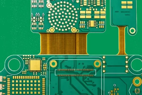
An 8-layer rigid-flex PCB stackup structure refers to a PCB structure composed of 8 conductive layers arranged in a specific sequence, where certain areas use rigid materials and other areas use flexible materials, all integrated together through a lamination process. In simple terms, it is not just a standard “8-layer board,” but a combination of “bendable flexible circuits” and “rigid circuits for component mounting” integrated into a single board.The advantage of this design is that the rigid sections are responsible for mounting chips, connectors, controllers, and other components, while the flexible sections bridge spaces and connect different modules, thereby reducing the risks caused by connectors, flat cables, and solder joints.
Why Is It Critical for Signal Integrity?
In high-speed electronic products, the key concern is not only whether signals can be transmitted, but whether they can be transmitted stably, accurately, and with low loss. An 8-layer stackup design can create stable reference planes by properly arranging power layers, ground layers, and signal layers, thereby reducing impedance fluctuation, reflection, crosstalk, and electromagnetic interference.Especially in high-frequency transmission, differential signals, RF signals, and high-speed digital signal applications, the rationality of the stackup structure directly determines whether the product performance is reliable.
Advantages and Features of 8-Layer Rigid-Flex PCB Stackup Design
| Advantage | Description |
| Connection reliability | Integrated connection between rigid and flexible layers reduces connectors and external wiring harnesses, improving overall stability |
| Fewer components | Compared with traditional rigid PCBs, it reduces some connectors, via transitions, and auxiliary wiring harnesses |
| Flexible design solutions | Meets highly complex, difficult routing, and space-constrained structural requirements |
| High-density applications | Flexible areas support fine-line routing, while rigid areas are suitable for high-density component installation |
| Smaller and lighter packaging | Integrated design reduces volume and weight while improving system integration |
How Is an 8-Layer Rigid-Flex PCB Stackup Designed?
Requirement Confirmation and Functional Partitioning
The first step in designing an 8-layer rigid-flex PCB is not drawing the board directly, but first dividing the functions: which areas require component mounting, which areas require bending, which signals are high-speed signals, and which areas must withstand mechanical stress.Only after defining the functional boundaries can the subsequent stackup, material selection, and routing planning become more reasonable. At this stage, it is also necessary to confirm board thickness, bending radius, connection methods, working environment, and target cost to avoid repeated modifications later.
Stackup Planning and Structural Design
Stackup design is one of the core parts of the entire project. Engineers usually determine the arrangement of signal layers, power layers, and ground layers first, then combine this with the distribution of flexible and rigid areas to plan the structure.
For 8-layer boards, a common approach is to place high-speed signal layers close to reference planes, allow power and ground layers to form stable shielding, and reduce critical traces crossing discontinuous reference planes. Flexible areas should avoid excessive vias and sharp bends to ensure bending life.
Routing Design and Manufacturability Inspection
Routing design must not only meet electrical requirements but also consider manufacturing feasibility. For example:
- Trace widths in flexible areas cannot be too narrow, otherwise they may crack due to bending fatigue;
- Vias cannot be placed too close to bending areas, otherwise mechanical damage may occur;
- The placement of BGAs, connectors, and other components must also consider assembly, rework, and heat dissipation.
After the design is completed, a DFM (Design for Manufacturability) inspection is required to confirm whether it meets factory manufacturing capabilities and reduce prototype failure risks.
Lamination, Drilling, Copper Plating, and Final Testing
The manufacturing stage generally includes multiple lamination cycles, drilling, hole metallization, circuit etching, profile machining, and final testing.Rigid-flex boards are more complex than standard PCBs because rigid and flexible materials have different thermal expansion coefficients. During lamination, temperature, pressure, and alignment accuracy must be strictly controlled.After production, continuity testing, impedance testing, visual inspection, and reliability verification are also required to ensure stable operation in real-world environments.
How to Improve Impedance Control and Signal Integrity in 8-Layer Stackup Design
Core Principles of Impedance Control
The essence of impedance control is maintaining continuous and stable electrical characteristics during signal transmission to reduce reflection and distortion.In 8-layer rigid-flex PCBs, high-speed signals typically use microstrip or stripline structures, and target impedance is achieved by controlling trace width, spacing, dielectric thickness, and copper thickness.
For differential pair routing, the spacing consistency between the two traces must also be controlled to ensure timing matching and common-mode noise suppression.Even slight deviations in stackup parameters may cause impedance to deviate from the target value, so simulation and actual manufacturing capability must be considered simultaneously during design.
Key Points for Signal Integrity Optimization
Signal integrity optimization mainly includes four aspects:
- Reduce signal traces crossing split ground or power planes to avoid discontinuous reference planes;
- Keep critical high-speed signals on the same layer, same direction, and same reference plane whenever possible to reduce vias;
- Match the lengths of clock lines and differential pairs when necessary to avoid timing deviation;
- Properly place decoupling capacitors and return paths near high-speed interfaces to reduce noise coupling.
For rigid-flex boards, special attention must be paid to local impedance changes caused by bending in flexible areas. Therefore, flexible trace width, copper thickness, and coverlay design must be handled more carefully.
Methods for Optimizing 8-Layer Stackup PCB Performance and Reducing Crosstalk
| Optimization Direction | Specific Method | Expected Result |
| Reasonable layer arrangement | Place signal layers close to complete ground planes, pair power and ground layers together | Improve return path stability |
| Control trace spacing | Maintain sufficient spacing between high-speed traces and sensitive traces | Reduce crosstalk |
| Reduce vias | Minimize layer transitions in critical links | Reduce reflection and parasitic inductance |
| Optimize reference planes | Avoid routing across split planes | Maintain impedance continuity |
| Differential pair matching | Control length, spacing, and symmetry | Improve high-speed transmission stability |
| Flexible area protection | Avoid sharp corners and dense vias in bending areas | Improve mechanical lifespan |
Why Do “Details” Determine Success or Failure?
Many customers believe that PCB design is simply drawing traces, but in reality, the invisible details are what truly affect product stability.For example, even with the same 8-layer board, an unreasonable stackup may cause high-speed signal jitter, packet loss, or bit errors. Improper flexible area design may lead to cracks or poor contact after prolonged use.For products requiring high reliability, technical details are not optional extras—they are the foundation of overall performance.
What Materials Should Be Used for 8-Layer Rigid-Flex PCBs?
Selection of Materials for Rigid Areas
Rigid sections usually use FR-4 series materials because they offer good mechanical strength, moderate cost, and mature manufacturing processes, making them suitable for component mounting and structural stability.If the product requires higher high-speed transmission, lower loss, or better high-frequency performance, lower-loss high-performance materials may be selected to reduce dielectric loss and signal attenuation.Material selection should balance performance, cost, and manufacturability rather than simply pursuing higher specifications.
Selection of Materials for Flexible Areas
Flexible sections usually use PI (polyimide) substrates because they provide excellent heat resistance, flexibility, and repeated bending durability.The thickness of flexible copper foil, coverlay materials, and adhesive systems also affect bending life and routing stability.If the flexible area requires dynamic bending, material requirements become stricter; if it only requires one-time assembly bending, a balance between reliability and cost can be considered.
Common Material Comparison Table
| Area | Common Material | Application Scenario | Features |
| Rigid substrate | FR-4 | General electronic products | Moderate cost, high strength, mature process |
| High-speed rigid area | Low-loss materials | High-speed communication and RF products | Low dielectric loss and more stable signals |
| Flexible substrate | PI | Flexible connections in rigid-flex boards | Heat resistant, bend resistant, highly reliable |
| Conductor material | Electrolytic copper / rolled annealed copper | Traces and pads | Excellent conductivity; rolled copper is better for flexible areas |
| Protective cover layer | Coverlay | Flexible circuit protection | Insulation, moisture resistance, and circuit protection |
Why Must Material Selection Consider the Operating Environment?
When selecting materials for an 8-layer rigid-flex PCB, the actual operating environment must be fully considered because different environments directly affect PCB stability, lifespan, and signal transmission performance.If only cost or basic parameters are considered while ignoring factors such as temperature, humidity, vibration, and bending frequency, problems such as trace cracking, delamination, unstable impedance, or even product failure can easily occur later.
For example:
- In industrial equipment or automotive electronics, where PCBs operate long-term under high temperature and vibration, materials with stronger heat resistance and higher mechanical stability are required;
- In wearable devices or foldable electronics, where flexible areas require repeated bending, PI flexible materials and rolled annealed copper with better bending performance are commonly used to extend service life;
- For high-speed communication equipment, dielectric constant and loss factor are equally important. Excessive dielectric loss can cause signal attenuation and data errors.
In addition, humid environments can affect insulation performance, so some applications also require moisture-resistant and corrosion-resistant materials.
Frequently Asked Questions
What Products Are Suitable for 8-Layer Rigid-Flex PCBs?
The question many customers care about most is not “What is it?” but “Can it solve my problem?”8-layer rigid-flex PCBs are especially suitable for products with compact space, complex routing, and multi-module connections, such as:
· High-end consumer electronics
· Industrial control motherboards
· Medical testing equipment
· Communication modules
· Automotive electronics
· Wearable devices
Because they reduce connectors and wiring harnesses while improving system integration, they also enable more efficient routing solutions within limited space.
For customers, this means:
· More compact product structures;
· Easier assembly;
· Fewer failure points;
· More stable long-term operation.
If your product has clear requirements for signal integrity, anti-interference capability, lightweight structure, and high reliability, an 8-layer rigid-flex PCB is usually more advantageous than a traditional rigid PCB.
Why Choose PCBSync 8-Layer Rigid-Flex PCBs?
PCBSync focuses on providing high-performance and highly reliable PCB solutions and can customize more suitable 8-layer rigid-flex PCB solutions according to different application scenarios.Whether for consumer electronics, industrial applications, or communication equipment, designs can be optimized around your structural, performance, and budget requirements.Our focus is not simply on “manufacturing a PCB,” but on helping customers consider manufacturability, reliability, and performance during the R&D stage so that products can move into mass production more smoothly and efficiently.
Manufacturer Warranty and Contact Support
We specialize in providing high-performance and highly reliable PCB printed circuit board solutions. Whether for consumer electronics, industrial applications, or communication equipment, we can customize the most suitable products according to your requirements.
You can send us your dimensions, layer count, impedance requirements, and application scenarios, and we will provide more suitable recommendations based on your actual needs to help you enter mass production faster.If you would like to learn how we can support your project, please contact us for professional advice.
WhatsApp: +86 13425156463
VK: vk.com/id1058761391
Email: [sales@toplinecircuit.com](mailto:sales@toplinecircuit.com)
Website: [www.toplinecircuit.com](http://www.toplinecircuit.com)
Address: 3rd Floor, Building B3, Yanchuan North Industrial Park, Yanluo Street, Bao’an District, Shenzhen, China


")

