


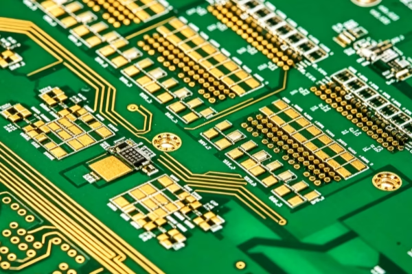
As electronic products continue to grow in complexity, traditional single-layer or multi-layer rigid PCBs can no longer meet the design requirements of modern devices. Especially in smartphones, AI servers, wearable devices, aerospace systems, and industrial control equipment, the demand for compact layouts and complex routing has made 10-layer rigid-flex PCBs an ideal solution.
What Is a 10-Layer Rigid-Flex PCB?
Overview of Rigid-Flex PCBs
A rigid-flex PCB, also known as a rigid-flex circuit board, is a type of printed circuit board technology that integrates rigid multilayer boards and flexible circuit boards into a single structure. Its main features include:The flexible section can bend and fold, providing support for complex routing;The rigid section can carry more electronic components and modules, ensuring circuit stability.
Why Rigid-Flex PCBs Are Popular?
| Advantage | Description |
| Multi-component integration | Multiple PCB assemblies and electronic components can be integrated into a single board, improving assembly efficiency |
| Flexible circuit support | The flexible section provides the necessary support structure for complex routing |
| Rigid module support | The rigid multilayer section serves as the foundation for modular designs and supports high-density electronic components |
| Space optimization | Saves installation space in compact devices and improves product design flexibility |
These characteristics make rigid-flex PCBs essential in high-end electronics, industrial control systems, and aerospace equipment. They are especially advantageous in applications requiring multilayer high-density routing, complex folding structures, or limited installation space.
Manufacturing Process of a 10-Layer Rigid-Flex PCB
PCB Design and Stack-Up Structure
The manufacturing process begins with circuit design, including the layout of rigid and flexible sections, signal routing for each layer, and power layer distribution. A typical stack-up structure includes:
- Flexible inner layers 1–2 used for signal routing and bending areas;
- Rigid layers 3–10 used for fixing modular components and high-density routing.
The precision of the stack-up design directly affects manufacturing stability and final board performance.
Material Preparation and Processing
The flexible circuit substrate uses high-temperature-resistant polyimide film, while the rigid section uses high-Tg FR4 material. The flexible and rigid sections are bonded together using specialized adhesives or prepreg materials while ensuring thickness consistency and optical flatness according to design specifications.
Etching and ENIG Surface Treatment
To ensure circuit precision and long-term reliability, 10-layer rigid-flex PCBs commonly use ENIG (Electroless Nickel Immersion Gold) surface treatment. Surface finishing after etching improves copper oxidation resistance and soldering reliability.
Rigid-Flex PCB Manufacturing Parameters
| Process Item | Specification |
| Finished thickness | Flexible: 0.2 mm, Rigid: 1.6 mm |
| Solder mask colors | Red, green, blue, black, white, Taiyo PSR4000 white |
| Copper thickness | 0.5 oz, 1 oz, 2 oz, 3 oz, up to 6 oz |
| PCB thickness range | 0.5 mm to 3.0 mm (0.02″ to 0.12″) |
| Silkscreen color | Black or white |
| Surface finish | ENIG, HASL, OSP |
| Layer count range | 1 layer to 20 layers |
These specifications can meet the design requirements of various high-performance electronic products.
Lamination and Profiling
After stack-up and etching are completed, the flexible and rigid sections undergo lamination under high temperature and pressure. This process tightly bonds the layers while maintaining the flexibility of the flexible section. Profiling and cutting are then performed to ensure dimensional consistency and precision for every PCB.
Testing and Quality Inspection
After fabrication, the board undergoes electrical testing and visual inspection. Key inspections include signal integrity, electrical continuity, and flexible bending life. These tests ensure that every 10-layer rigid-flex PCB meets high-performance and high-reliability standards.
How to Improve Rigid-Flex PCB Performance?
Reliability of Rigid-Flex Structures
The flexible section must withstand repeated bending without conductor breakage, while the rigid section must support modular components. Key technologies include:
- Precise control of flexible layer thickness;
- Use of high-performance polyimide materials;
Use of high-Tg FR4 materials in rigid sections for improved heat and mechanical resistance.
Signal Integrity and EMC Performance
In 10-layer rigid-flex PCBs, high-speed signal lines require proper impedance matching and electromagnetic shielding. This can be achieved through:
- Tight coupling between signal layers and power planes;
- Adding ground planes in critical areas;
- Avoiding signal line cross-interference.
High-Density Assembly Capability
Rigid-flex PCB designs allow large components and modules to be mounted on rigid sections while flexible sections provide foldable interconnections, saving space. Proper layout planning improves assembly efficiency and reduces soldering defects.
Precision Manufacturing Control
Because 10-layer rigid-flex PCBs are thin and contain many layers, strict control of copper thickness and lamination pressure is required. Maintaining tolerances within ±0.05 mm is essential for ensuring manufacturing precision.
How to Choose Materials for Rigid-Flex PCBs?
Flexible Section Materials
Polyimide film: High heat resistance and excellent flexibility, suitable for folding and bending applications;
Polyester film (PET): Lower cost and good chemical resistance, suitable for general folding or short-term applications.
Rigid Section Materials
High-Tg FR4 material: Excellent heat resistance and rigidity, suitable for high-density component mounting;
Heavy copper materials: Suitable for high-current applications, with copper thickness up to 6 oz.
Surface Finish and Solder Mask
ENIG: Excellent solderability and oxidation resistance;
HASL: Lower cost and suitable for general applications;
OSP: Environmentally friendly surface finish suitable for precision soldering.
Available solder mask colors include red, green, blue, black, white, and Taiyo PSR4000 white to match customer appearance requirements.
Lamination Materials and Adhesives
Selecting suitable flexible adhesives and lamination films, such as acrylic- or epoxy-based materials, ensures that the flexible and rigid sections will not delaminate or warp under high-temperature and high-humidity conditions.
Frequently Asked Questions
Why Choose a 10-Layer Rigid-Flex PCB Instead of a Standard Multilayer PCB?
A 10-layer rigid-flex PCB enables high-density routing within limited space while combining flexible folding capability with rigid module support. Compared with standard multilayer PCBs, it offers:Reduced internal device space requirements and improved compact design efficiency;Support for high-density routing and complex component installation;Improved electronic product reliability and service life;Compatibility with high-end applications such as aerospace, smartphones, and wearable devices.(If you are involved in AI servers, industrial control systems, or precision electronic products, rigid-flex PCBs are undoubtedly one of the best solutions for improving product performance and design flexibility.)
A 10-layer rigid-flex PCB is a high-performance PCB solution that integrates high-density routing, modular support, and flexible folding into a single structure. It not only saves space and improves electronic integration but also ensures circuit stability and reliability.During manufacturing, precise stack-up design, ENIG surface treatment, high-performance material selection, and strict quality control ensure that every board meets the requirements of high-end electronic products.Choosing the right 10-layer rigid-flex PCB is essential for improving electronic product performance, reducing assembly costs, and enhancing reliability. By integrating flexible circuits and rigid circuit modules into a modular structure, rigid-flex PCBs not only save space but also optimize electrical performance for demanding applications.
Whether you are designing smartphones, AI servers, or industrial control systems, we can customize the most suitable 10-layer PCB solution for your needs, including FR4 multilayer boards, HDI boards, heavy copper PCBs, and rigid-flex PCBs. We also provide multiple surface finishes such as ENIG, HASL, and OSP, along with various solder mask and silkscreen color options to ensure optimal product performance and appearance.For customization or technical consultation, please contact us for professional advice and quotations:
WhatsApp: +86 13425156463
VK: vk.com/id1058761391
Email: [sales@toplinecircuit.com](mailto:sales@toplinecircuit.com)
Website: [www.toplinecircuit.com](http://www.toplinecircuit.com)
Address: 3F, Building B3, Yanchuan North Industrial Park, Yanluo Street, Bao’an District, Shenzhen, China


")

