


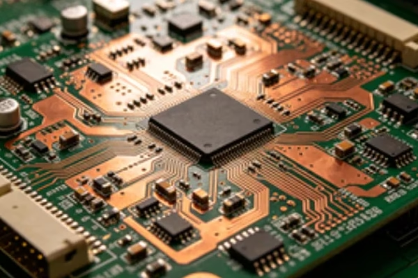
With the popularization of smart homes, devices such as smart speakers, smart door locks, and sensors have entered thousands of households. As the core component of these devices, the PCB (Printed Circuit Board) directly affects the stability and service life of the equipment. Tailored to the characteristics of smart home devices—small size, energy saving, and integrated functions—this exclusive PCB manufacturing solution not only ensures product performance but also controls costs and improves mass production efficiency, helping enterprises seize the market.

Core Adaptation of the Solution: Meeting Smart Home Scenario Needs
The manufacturing of smart home PCBs needs to match the usage needs of different devices, optimize process parameters, and achieve the unity of adaptability, practicality, and economy, focusing on three core adaptation directions:
- Miniaturization: For small devices (e.g., smart sensors), use small PCBs with BGA/QFN packages, high-precision machines and AOI/X-ray inspection to avoid soldering issues.
- Low Power Consumption: For battery-powered devices, choose low-loss substrates and thin copper foil, and test to ensure long battery life.
- Communication: Support Wi-Fi/Bluetooth, separate circuit areas, add shields, and lay short RF lines for stable communication.
- Environmental Compliance: Meet RoHS 2.0, use lead-free/halogen-free substrates, control emissions and pass environmental certifications.
- Mass Production Compatibility: Support small-batch samples and large-batch production with stable quality and no batch rework.
Core Advantages of the Solution: Fully Empowering Smart Home Enterprises
Targeting the pain points of the smart home industry, this solution has obvious advantages in quality, efficiency, cost, and customization, as shown in the following table:
| Advantage Type | Specifics | Value |
| Quality Assurance | Full-process control, 99.99% yield, international certifications. | Stable quality, less rework. |
| Efficiency | Samples in 6h, small batches in 24h, one-stop service. | Fast new product launch, timely response. |
| Cost Control | 10%-15% lower quotation, high yield reduces rework cost. | Lower cost, better cost performance. |
| Customization | Customizable size/layers, supports high-end PCB manufacturing. | Meets personalized needs, unique products. |
Common Problems and Solutions in Smart Home PCB Manufacturing
Combined with practical production experience, two common problems are sorted out, and simple and easy-to-operate solutions are given to ensure stable PCB quality:
- Soldering Defects: Use high-precision machines and quality solder paste, calibrate equipment, set proper temperature, and inspect after soldering.
- Signal Interference: Properly divide circuits, add shields and optimize RF lines for stable wireless communication.
- Improper Substrate Selection: Choose temperature/moisture-resistant substrates and test performance in advance.
- Unreasonable Circuit Layout: Plan circuits by function, control line spacing and avoid cross-overlapping for smooth conduction.
PCB Quality Control Process: Building a Solid Product Quality Line
Quality control is the core of smart home PCB manufacturing, running through the entire production process, which is simple and easy to operate and suitable for mass production needs. Before production, strictly screen raw materials such as substrates and solder paste to prevent unqualified materials from entering the factory; during production, set inspection nodes for each process, focusing on key parameters such as placement accuracy and soldering temperature to avoid human errors; after production, conduct triple inspections including AOI automatic inspection, X-ray inspection, and power-on test to check various problems such as solder joints, signals, and conduction, ensuring that each PCB meets the standards, avoiding batch quality hazards, and establishing a quality traceability system to quickly locate the cause and rectify it in time if problems occur.
Solution After-Sales Guarantee: Fully Escort Enterprise Production
Targeting the production pain points of smart home enterprises, provide comprehensive after-sales guarantee to reduce enterprise production risks. If quality problems occur during mass production, respond to after-sales needs within 24 hours, arrange professional personnel to connect, and quickly troubleshoot problems and rework; provide technical consulting services to answer questions such as PCB design and process optimization one-on-one, helping enterprises solve production difficulties; support sample rework and batch rework services, and provide long-term technical support to cooperate with enterprises in product iteration and upgrading, fully ensuring the smooth progress of enterprise production without worrying about subsequent after-sales hazards.