


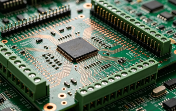
In the field of industrial automation, the Programmable Logic Controller (PLC) serves as the core control unit, and its communication backplane PCB board is a key carrier connecting the CPU module, I/O module, and communication module. It undertakes the core functions of high-speed data transmission, stable signal conduction, and power distribution. The rationality of the PLC communication backplane PCB board design directly determines the response speed, anti-interference ability, and long-term operational reliability of the PLC system. Especially in complex industrial environments, it is necessary to balance signal integrity, electromagnetic compatibility, and structural adaptability to create a customized solution for different industrial scenarios.
Core Design Requirements of PLC Communication Backplane PCB Board
The design of the PLC communication backplane PCB board must be based on the harsh requirements of industrial scenarios, combined with the PLC system’s communication protocol, module expansion needs, and operating environment, and the core design requirements are as follows:
- Signal Transmission: Support mainstream industrial buses such as PCIe, EtherCAT, Modbus, and Profibus DP, with a transmission delay ≤ 1ms and a bit error rate lower than 10⁻⁹ to meet the needs of real-time industrial control.
- Anti-interference: Resist electromagnetic interference (EMI) generated by industrial equipment such as motors and frequency converters, with a radiation immunity ≥ 30V/m and a conducted immunity ≥ 10V, complying with the IEC 61000-6-2 standard.
- Expansion Adaptability: Adopt a multi-slot design, compatible with CPU, digital I/O, analog I/O, and communication modules, supporting hot swapping (under compatible systems) to facilitate on-site maintenance and system expansion.
- Reliability: Adapt to a wide temperature range of -20℃~70℃, with a Mean Time Between Failures (MTBF) ≥ 50,000 hours, and have corrosion resistance, vibration resistance, and aging resistance.
- Power Distribution: Support single or dual redundant power input, with a power fluctuation ≤ 5%, stably providing standard power supplies such as 3.3V, 5V, and 12V for each module.
Key Design Scheme of PLC Communication Backplane PCB Board
Combined with the core design requirements, a high-reliability and high-compatibility PLC communication backplane PCB board scheme is created from five core dimensions: substrate selection, stack-up design, wiring optimization, impedance control, and grounding design, ensuring the feasibility and practicality of the scheme.
Substrate Selection: Balancing Stability and Environmental Adaptability
As the foundation of the PCB board, the substrate directly affects signal transmission quality and environmental adaptability. It is necessary to select industrial-grade special substrates according to the operating environment, and the specific selection standards and parameters are shown in the following table:
| Selection Dimension | Recommended Material | Core Parameters | Application Scenarios |
| General Industrial Scenarios | High Tg FR-4 | Tg=170℃, CTE 13ppm/℃, PCB thickness 2.0mm, copper thickness 1oz | General manufacturing, municipal engineering, light industry |
| Harsh Industrial Scenarios | Rogers 4350 | Tg=150℃, low dielectric loss, salt spray resistance for 500 hours, flame retardant grade UL94-V0 | Chemical industry, metallurgy, water treatment |
| High-Speed Communication Scenarios | Isola FR408 | Stable dielectric constant, low signal attenuation, supporting high-speed transmission above 10Gbps | Industrial Ethernet, TSN time-sensitive network |
The surface of the substrate is treated with an immersion gold process, with a gold layer thickness ≥ 0.5μm, which improves the plug-in resistance of the pad (≥ 1000 times) and enhances oxidation resistance, avoiding poor contact during long-term operation. The PCB surface is coated with a 30μm thick silicone conformal coating to further improve corrosion resistance and moisture resistance.
Stack-Up Design: Ensuring Signal Shielding and Transmission Stability
The PLC communication backplane PCB board adopts a multi-layer structure design to realize signal shielding, impedance matching, and stable power distribution. According to the communication rate and module quantity, a 6-layer or 8-layer structure is recommended, and the typical structure of the 8-layer board is as follows:
| Layer Number | Layer Type | Core Function | Design Points |
| 1 | Signal Layer | Transmitting high-speed bus signals (PCIe, EtherCAT) | Close to the ground plane, avoiding cross-layer jumps |
| 2 | GND Layer | Providing signal shielding and return path | Keep the plane intact without slots or breakpoints |
| 3 | Signal Layer | Transmitting I/O control signals | Isolated from analog signal layers to avoid interference |
| 4 | Power Layer | Distributing 3.3V, 5V, 12V power supplies | Closely coupled with the ground plane to reduce power noise |
| 5 | GND Layer | Reference plane, suppressing electromagnetic interference | Adjacent to the power layer to enhance shielding effect |
| 6 | Signal Layer | Transmitting low-speed control signals | Keep away from high-speed signal layers to reduce crosstalk |
| 7 | GND Layer | Auxiliary shielding, reducing inter-layer crosstalk | Closely adjacent to the signal layer to shorten the return path |
| 8 | Signal Layer | Transmitting power control signals | Loose wiring to avoid crossing with high-speed signals |
The core principle of stack-up design: High-speed signal layers are closely adjacent to the ground plane to ensure short and stable signal return paths; power layers and ground layers are arranged in pairs to reduce power noise affecting signals; different types of signals are arranged in separate layers to avoid cross-interference.
Wiring Optimization: Improving Signal Integrity and Anti-Interference Ability
Wiring design is the core of the PLC communication backplane PCB board, which needs to follow strict rules according to the signal type and transmission rate to reduce signal reflection, crosstalk, and attenuation. The specific optimization points are as follows:
- Differential Signal Wiring: High-speed buses (PCIe, EtherCAT) adopt differential pair wiring, strictly controlling the length difference ≤ 0.5mm to ensure synchronous signal arrival at the receiving end; the distance between differential pairs meets S ≥ 3W (W is the wiring width) to avoid crosstalk.
- Signal Isolation Wiring: Digital signals and analog signals are wired separately, with a distance ≥ 5mm; analog signal wiring length ≤ 5cm, with grounding copper foil set on both sides to form a shielding slot, reducing noise interference (analog signal noise ≤ 8μV).
- Via Optimization: Reduce the number of vias for high-speed signals, use back-drilling technology to remove residual copper, reduce parasitic inductance and capacitance, and avoid impedance discontinuity.
- Power Wiring: The width of the power line ≥ 1.5mm, adjusted according to the current size; a decoupling capacitor is arranged near each IC, close to the pin, with a wiring length ≤ 1.27mm to filter power noise.
Impedance Control: Matching High-Speed Signal Transmission Requirements
In high-speed signal transmission, impedance mismatch will cause signal reflection and attenuation, affecting transmission quality. It is necessary to strictly control the characteristic impedance of PCB wiring according to different bus types. The common bus types and impedance requirements are shown in the following table:
| Bus Type | Typical Impedance Requirement | Control Method | Tool Support |
| PCIe | 85Ω ±10% (Differential) | Adjust wiring width, dielectric thickness and copper thickness, adopt stripline structure | Polar SI9000, Altium Designer |
| Ethernet (1000BASE-T) | 100Ω (Differential) | Control differential pair spacing, avoid line width mutation | Cadence Sigrity, HyperLynx SI |
| USB 2.0 | 90Ω (Differential) | Adopt microstrip line structure, close to the ground plane | Polar SI9000 |
| CANopen | 120Ω (Differential) | Set terminal resistors at both ends of the bus, control wiring length ≤ 10m | Altium Designer |
The core of impedance control: Keep the wiring width consistent in the same grid to avoid impedance discontinuity caused by line width mutation; high-speed signal wiring avoids crossing split areas to ensure a stable signal return path.
Grounding Design: Suppressing Electromagnetic Interference
Reasonable grounding design can effectively suppress electromagnetic interference, reduce ground bounce effect, and ensure stable signal transmission. The key design points are as follows:
- Partitioned Grounding: Digital ground, analog ground, and shield ground are designed separately to form independent grounding loops to avoid mutual interference; they are converged at a single point near the system ground, with a grounding impedance ≤ 0.05Ω.
- Ground Plane Design: Keep the ground plane intact, without slots or breakpoints, to provide a stable return path for high-speed signals; fill the blank area of the PCB with grounding copper to avoid the “antenna effect”.
- Shield Grounding: A metal shield cavity is set in the analog I/O area, with a shielding effectiveness ≥ 40dB; the shield is reliably connected to the system ground to reduce external interference coupling.
PLC Communication Backplane PCB Board Test and Verification Scheme
After the scheme is implemented, strict test and verification are required to ensure that the PCB board meets the design requirements and guarantees the stable operation of the PLC system. The test content covers four dimensions, and the specific test items and standards are as follows:
- Electrical Performance Test: Measure the I/O interface voltage fluctuation ≤ 5%, analog signal acquisition accuracy ≥ 0.08%, power distribution efficiency ≥ 95%; measure S parameters with a Vector Network Analyzer (VNA) to verify impedance matching effect; test signal transmission delay ≤ 1ms, bit error rate lower than 10⁻⁹.
- Environmental Adaptability Test: Cycle 100 times within the temperature range of -20℃~70℃ without failure; no solder joint detachment or line breakage in the vibration test (10-2000Hz); no corrosion or performance degradation in the salt spray test (5% NaCl solution) for 500 hours; normal operation in the humidity test (85%RH, 40℃) for 1000 hours.
- Signal Integrity Test: Measure signal waveforms with an oscilloscope, check impedance matching through Time Domain Reflectometry (TDR) analysis; evaluate signal jitter and quality through eye diagram analysis; ensure adjacent signal crosstalk ≤ -35dB through crosstalk analysis.
- Reliability Test: MTBF test ≥ 50000 hours, continuous operation for 720 hours without failure; plug-in resistance test ≥ 1000 times, no pad detachment and good contact; no significant attenuation of electrical performance after the aging test (70℃, 1000 hours).
Scheme Advantages and Application Scenarios
This PLC communication backplane PCB board scheme has four core advantages through comprehensive optimization and strict test verification, and the specific points are as follows:
- High-Speed Transmission Advantage: Support multi-protocol high-speed communication, ensure fast data interaction between modules, and meet real-time control needs.
- Strong Anti-Interference Advantage: Multiple optimization designs can resist industrial electromagnetic interference and ensure stable signal transmission.
- High Reliability Advantage: Adapt to wide temperature, corrosion resistance and vibration resistance, ensuring long-term continuous operation.
- Flexible Expansion Advantage: Multi-slot design, support module hot swapping and flexible expansion, adapt to different scale PLC systems.
The above advantages make the scheme widely applicable to various industrial automation scenarios, including electric power, chemical industry, metallurgy, water treatment, municipal engineering, manufacturing, etc. It can be adapted to small, medium and large PLC systems, providing stable and efficient communication backplane support for both single-machine control and distributed control.