In PCB design, the layout of power and ground lines directly affects circuit stability and signal quality. Improper handling can easily lead to noise interference, voltage fluctuations, and signal distortion. A well-planned power path and ground structure can significantly improve system reliability and make circuit operation more stable.

The Importance of Power and Ground Layout
Power supplies provide energy to the circuit, while ground lines form the current loop; together, they determine the stability of the electrical environment. An unreasonable power path design can lead to voltage drops or uneven power supply; an incomplete ground layout can cause chaotic return paths, resulting in interference problems. These problems are more pronounced in high-frequency or high-power circuits, therefore, the arrangement of power and ground lines needs to be carefully considered during the design phase.
Power Trace Design Principles
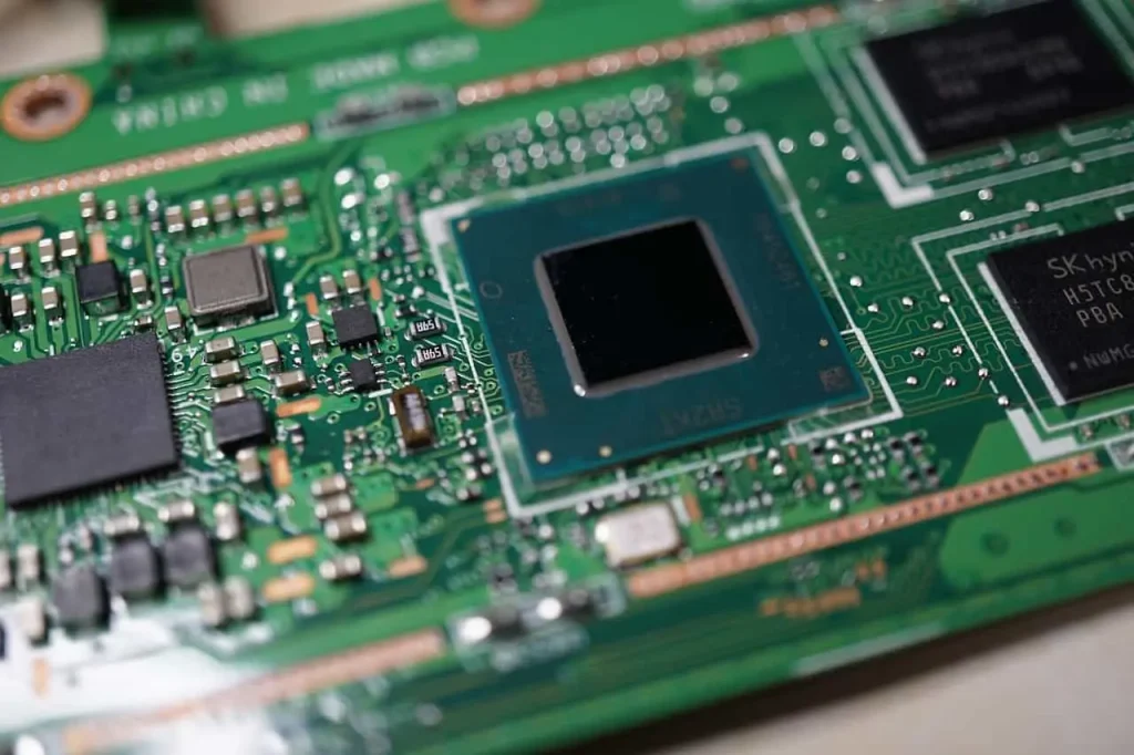
Power traces need to have low impedance characteristics to ensure stable current transmission. The design should minimize trace length and avoid excessive bends to reduce losses. Trace width should be adjusted according to the current magnitude; high-current lines require wider traces to reduce the risk of overheating. In multilayer board design, independent power planes can be used to improve power supply stability while reducing interference to signal planes.
Ground Layout and Return Path Optimization
Ground lines not only handle current return but also affect overall anti-interference capability. During design, the ground plane should be kept as intact as possible, avoiding segmentation or interruption. A continuous ground plane provides a stable return path and reduces signal noise. In critical areas, such as near high-speed signals or sensitive circuits, ground lines should be tightly coupled to form a good shielding effect. A reasonable ground layout can effectively reduce electromagnetic interference.
Key Layout Techniques and Precautions
In practical design, the following techniques can be combined to optimize power and ground layout:
- Layered design of power and ground lines: Using independent layers improves stability and anti-interference capability.
- Reduce loop area: Shorten signal paths and reduce interference generation.
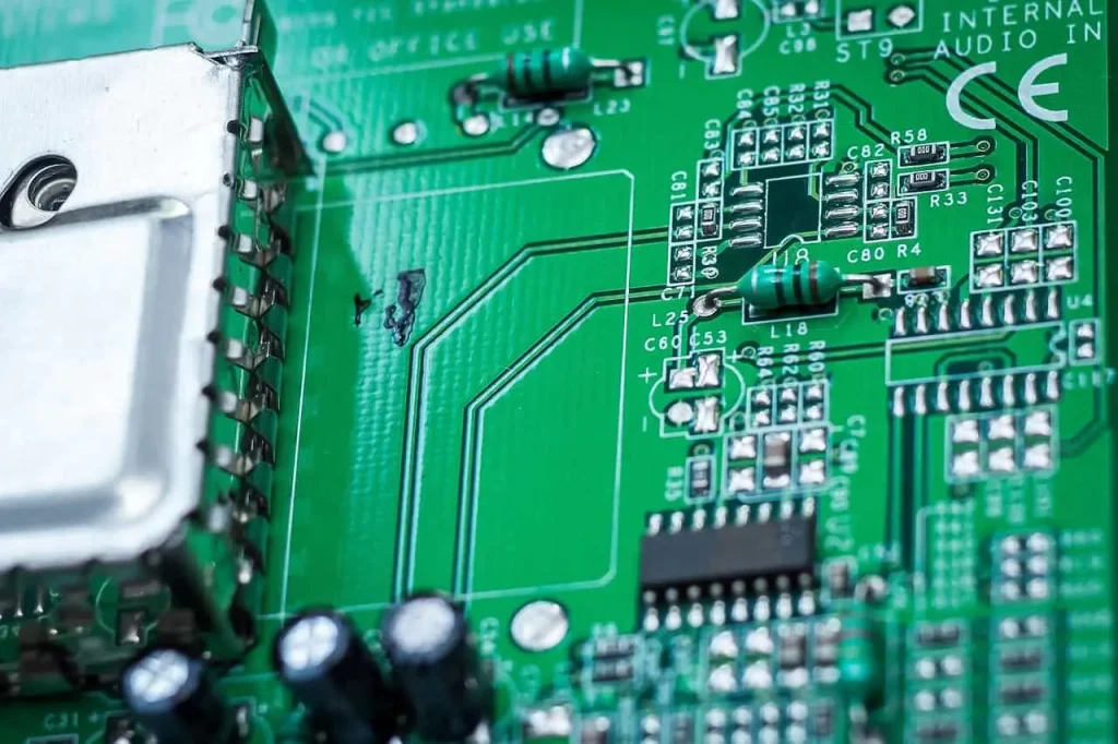
- Reasonable placement of decoupling capacitors: Place them close to chip power pins to improve power supply quality.
- Avoid ground line segmentation: Maintain continuity to ensure a smooth return path.
- Control power supply noise propagation: Reduce interference diffusion through reasonable wiring.
These techniques can effectively improve circuit performance.
Common Problems and Optimization Strategies
Common problems encountered during the design process include excessive power supply voltage drop, ground noise interference, and signal instability. These issues can be addressed by increasing power line width, optimizing ground plane structure, and adjusting layout. For high-frequency circuits, multi-point grounding or zoned grounding can be used to reduce interference. Through continuous design optimization, circuit stability and reliability can be gradually improved.
Power and ground layout is a critical aspect of PCB design. Properly planning traces and structures can effectively reduce interference and improve circuit performance. Continuously optimizing design details contributes to achieving more stable and reliable electronic systems.