PCB design is a crucial process for translating circuit principles into a usable industrial circuit board. A well-designed PCB not only ensures proper circuit operation but also enhances stability and interference resistance. For beginners, mastering clear design steps and key techniques can effectively reduce errors and improve design efficiency.
Clarifying Circuit Requirements and Functional Planning
Before starting PCB design, a clear understanding of the circuit’s function is essential, including input/output relationships, signal types, and power requirements. Dividing the circuit into functional modules helps ensure a more organized layout and routing later. Planning interface locations and structural dimensions in advance avoids space constraints after design completion. Clearly defining requirements is fundamental to the entire design process and helps reduce repeated modifications.
Schematic Design and Component Selection
The schematic is the starting point of PCB design, used to express circuit connections. During the drawing process, appropriate components need to be selected, ensuring that the symbols match the actual components. Connections should be clear and unambiguous, avoiding omissions or duplicate connections. Component parameters need to meet actual usage requirements, such as voltage levels and power requirements. A standardized schematic provides a reliable basis for subsequent design.
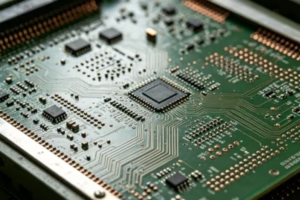
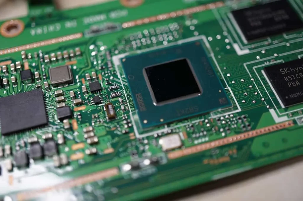
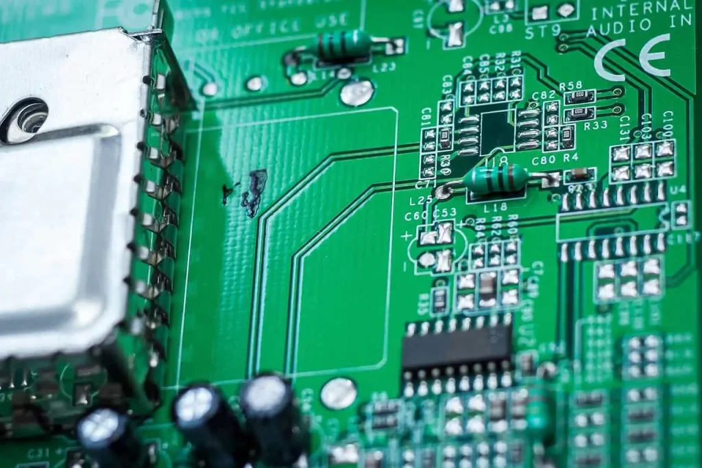
PCB Layout Design Techniques
Layout is the process of rationally placing components on a circuit board, directly affecting circuit performance and routing difficulty. During design, it’s necessary to partition the board according to functional modules, keeping related components as close as possible to reduce signal transmission distance. High-frequency devices should be placed near signal sources, and power devices require adequate heat dissipation space. Interface components should be placed near the board edge for easy connection and installation. A reasonable layout can improve the overall design quality.
Routing Rules and Key Operational Points
The routing stage requires completing electrical connections and ensuring stable signal transmission. In actual operation, pay attention to the following details:
- Keep the lines simple: Minimize corners and loops to improve signal transmission efficiency.
- Set appropriate trace widths: Widen power lines appropriately to ensure stable current transmission.
- Reduce via usage: Too many vias increase impedance and affect signal quality.
- Differentiate between different signal lines: Separate high-speed and low-speed signals to reduce interference.
- Optimize grounding design: Maintain continuous ground lines to improve anti-interference capabilities.
These operations can significantly improve the reliability and stability of the PCB.
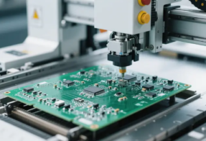
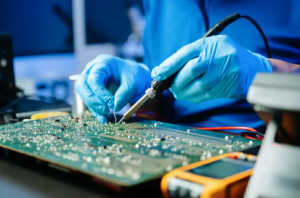
Inspection, Optimization, and Production Document Output
After design completion, a comprehensive inspection is required, including connectivity testing, spacing checks, and rule verification. The design rule checking function can identify potential problems early, preventing production errors. After inspection, production documents, such as Gerber files and drill files, need to be generated for actual manufacturing. An optimized and confirmed design better meets production and usage requirements.
PCB design involves steps such as requirements planning, schematic drawing, layout and routing, and inspection and optimization. Through standardized operations and continuous practice, design capabilities can be gradually improved, enabling the circuit board to achieve higher levels of performance and stability.