
Controlled impedance is not created by trace width alone. In a multilayer PCB, the stack-up determines how signal layers, reference planes, copper thickness, and dielectric materials work together.
A trace can look correct in the layout but still miss its impedance target if the finished board structure changes. Small differences in dielectric thickness, copper weight, resin flow, or layer arrangement can affect the final electrical result.
For projects with high-speed interfaces, differential pairs, RF paths, or sensitive timing requirements, stack-up review should happen before fabrication release. The goal is not only to choose a layer count. It is to define a structure that gives the required signal behavior and can be manufactured consistently.
Why Stack-Up Matters for Controlled Impedance
A multilayer PCB stack-up defines the relationship between copper layers and dielectric materials. It shows where signal layers, power layers, ground planes, cores, and prepreg materials are located.
For controlled impedance routing, this structure affects the electromagnetic field around each trace. The signal does not travel through the copper path alone. It also depends on the surrounding dielectric material and the nearby reference plane.
A stack-up should answer several basic questions:
- Which layers carry high-speed or controlled impedance signals?
- Which layers provide the closest reference planes?
- What dielectric thickness separates the trace from its reference plane?
- What copper thickness is expected after fabrication?
- Which material family will be used?
- Are differential pairs routed on the same layer?
- Are vias changing the signal path between layers?
When these points are unclear, impedance values may be difficult to predict or verify.
For projects that require multilayer fabrication support, see the Multilayer PCB product page. For impedance-focused manufacturing review, link relevant wording to Impedance Controlled PCBs.
Stack-Up Elements That Affect Impedance
Several stack-up factors work together. Changing one item can affect the final impedance result.
| Stack-Up Element | Why It Matters | What Buyers Should Confirm |
|---|---|---|
| Dielectric thickness | Changes the distance between trace and reference plane | Core and prepreg thickness for each controlled layer |
| Copper thickness | Changes trace geometry and field distribution | Finished copper requirement, not only starting copper |
| Material properties | Affects signal propagation and loss behavior | Material family and applicable electrical requirements |
| Reference plane position | Supports signal return paths | Ground or power reference near controlled layers |
| Trace geometry | Affects single-ended and differential impedance | Trace width, spacing, and copper profile assumptions |
| Layer arrangement | Affects routing options and return paths | Which layers carry critical signals |
| Via transitions | Can interrupt the signal path | Layer changes, via type, and return path continuity |
The table does not replace engineering review. It helps identify which inputs should be defined before production planning.
Dielectric Thickness and Reference Plane Distance
The distance between a signal trace and its reference plane is one of the most important impedance inputs.
A trace routed close to a reference plane behaves differently from the same trace routed farther away. When the dielectric thickness changes, the trace width often needs to change as well to maintain the same target impedance.
This matters for both single-ended and differential routing.
Do not rely on a generic trace width
A trace width used on one stack-up may not work on another. For example, a width selected for a thin dielectric layer may produce a different impedance if the same trace is placed above a thicker prepreg structure.
The PCB layout should be reviewed against the proposed production stack-up. A routing rule from an earlier project should not be copied without checking the new material and layer structure.
Keep critical signals close to a stable reference plane
High-speed and controlled impedance signals usually need a clear reference plane nearby. This supports a predictable return path and helps reduce unwanted coupling with other signals.
A signal layer without a nearby and continuous reference plane can create signal integrity problems even when the trace width appears correct.
Copper Thickness and Finished Trace Geometry
Copper thickness affects more than current capacity. It also changes the final geometry of controlled impedance traces.
During fabrication, copper features are processed through imaging, etching, plating, and surface treatment steps. The finished trace profile may differ from the shape shown in the original layout file.
For impedance-critical routing, the manufacturer may need to review:
- Starting copper thickness
- Finished copper thickness
- Trace width after processing
- Trace spacing for differential pairs
- Copper distribution across the panel
- Surface finish requirements
- Any special plating requirements
Finished copper matters more than nominal copper
A stack-up note should clearly identify whether copper values refer to base copper, finished outer-layer copper, or total copper after plating. Unclear copper notes can lead to different assumptions during impedance calculation.
Copper balance can affect manufacturing stability
Large differences in copper coverage between layers may affect lamination behavior, etching consistency, and board flatness. This does not always make a design unmanufacturable, but it should be reviewed before release.
For designs with higher current paths or heavier copper requirements, link relevant wording to Heavy Copper PCBs.
Material Selection and Electrical Consistency
The material system used in a multilayer PCB affects the dielectric environment around controlled traces.
Standard FR4 may be suitable for many digital and industrial applications. However, some projects require more specific electrical or thermal behavior. In these cases, the material direction should be defined before the stack-up is finalized.
Material selection may depend on:
- Signal speed
- Operating frequency
- Thermal exposure
- Assembly temperature profile
- Board thickness target
- Moisture sensitivity concerns
- Electrical loss requirements
- Customer material approval requirements
Do not specify only “FR4” when the project has electrical targets
“FR4” describes a broad material category. It does not fully define dielectric behavior, thermal properties, resin content, or process compatibility.
When a design requires controlled impedance, high-speed performance, or repeat production consistency, the material family should be reviewed with the stack-up instead of being treated as a generic line item.
For higher temperature project requirements, link relevant wording to High Tg PCB. For RF, microwave, or low-loss material discussion, link relevant wording to High Frequency PCB.
Layer Order and Signal Return Paths
Layer order affects how signals move across the board and how their return currents travel.
A controlled trace needs more than a target width. It also needs a stable reference plane. In many multilayer designs, this means placing critical signal layers adjacent to a ground plane or another suitable reference plane.
Avoid routing critical signals across split reference areas
A return current normally follows the path beneath or near the signal trace. If the reference plane is split, cut away, or interrupted, the return path may be forced to take a longer route.
This can increase noise, coupling, or timing problems. It may also make the impedance behavior less predictable.
Separate sensitive signal paths from noisy power regions
Critical signals should be reviewed against nearby power planes, switching regions, connectors, and high-current traces. The goal is not to isolate every signal completely. The goal is to identify routing areas that need more controlled layer planning.
Confirm the function of each layer
A useful stack-up note should identify whether each layer is intended for signal routing, ground reference, power distribution, shielding, or mixed use. This helps the layout team and manufacturer understand the purpose of the structure.
Differential Pair Routing Considerations
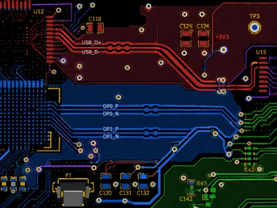
Differential pairs are common in high-speed digital interfaces and communication systems. Their behavior depends on both the individual traces and the relationship between the two traces.
The stack-up must provide enough information to calculate the required width and spacing.
Pair spacing should match the selected stack-up
The spacing between two traces affects differential impedance and coupling. A pair spacing that works on one layer may not work on another layer with a different dielectric height or copper thickness.
Keep the pair environment consistent
Differential pairs should avoid unnecessary changes in reference plane, layer transition, width, spacing, and nearby copper environment. Changes may be required by the layout, but they should be reviewed as part of the signal path.
Review layer transitions carefully
When a differential pair changes layers through vias, the transition can affect impedance and return current behavior. The impact depends on the via arrangement, reference planes, unused via stubs, and nearby ground return vias.
For dense routing, fine-pitch parts, microvias, blind vias, or BGA breakout structures, link the relevant wording to HDI PCBs.
Common Stack-Up Problems Before Fabrication
Some stack-up issues are easy to miss because they may not appear directly in Gerber files.
The stack-up is missing from the quotation package
Gerber data can show copper layers and drill information, but it may not define the required dielectric structure. For controlled impedance projects, a stack-up note should be included or requested during engineering review.
The impedance target is listed without routing information
An impedance note alone is not enough. The manufacturer may also need trace width, spacing, layer assignment, reference plane information, and material requirements.
The design uses an old stack-up from another project
A previous stack-up may not match the new board thickness, layer count, copper requirement, component layout, or material selection. Reusing it without review can create incorrect impedance assumptions.
Critical routing crosses plane splits or voids
A signal can lose its expected return path when it crosses a split ground region, slot, cutout, or copper void. This issue should be checked during layout and stack-up review.
Assembly requirements are reviewed too late
BGA packages, fine-pitch components, thermal pads, connectors, and test access can affect the PCB structure. For PCBA projects, the stack-up should be reviewed with the BOM and assembly requirements.
For BOM, pick-and-place data, assembly drawings, or test planning, link relevant wording to PCBA processing.
What Buyers Should Prepare Before Stack-Up Review
A complete package helps the manufacturer understand which stack-up details are critical.
| File or Requirement | Why It Is Needed |
| Gerber files | Shows routing layers, copper features, pads, and board outline |
| Drill files | Defines plated and non-plated hole requirements |
| Fabrication drawing | Provides board notes, dimensions, and special requirements |
| Stack-up notes | Defines intended layer arrangement and material structure |
| Impedance table | Identifies target values and controlled layers |
| Material requirements | Clarifies thermal, electrical, or customer-approved material needs |
| Board thickness requirement | Helps define core and prepreg structure |
| Assembly data, if applicable | Helps review BGA, thermal, test, and component requirements |
For Gerber files, drill files, fabrication notes, design review, or engineering changes, link the relevant wording to PCB design.
How to Verify Stack-Up Decisions Before Production
A stack-up review should end with clear information that can be checked.
Before production release, confirm:
- The controlled layers are identified
- Reference planes are defined
- Material direction is agreed
- Finished board thickness is confirmed
- Copper thickness assumptions are clear
- Trace width and spacing match the reviewed stack-up
- Differential pair rules are identified
- Via transitions are reviewed where relevant
- Impedance requirements are included in project documentation
- Assembly restrictions are known for PCBA projects
The final fabrication package should match the reviewed structure. A stack-up change after layout release can affect impedance calculations, routing rules, and production planning.
Preparing for Production Review
Controlled impedance depends on the interaction between layout, stack-up, materials, copper geometry, and manufacturing process. A multilayer design should not be released based only on layer count or a generic trace-width rule.
Before quotation or production release, send the Gerber files, drill data, stack-up notes, impedance requirements, finished thickness target, and material requirements for review. For PCBA projects, include the BOM, pick-and-place file, assembly drawing, and testing requirements where applicable.
For engineering review and quotation support, please send your Gerber files and BOM to sales@toplinecircuit.com.