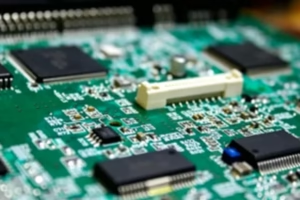
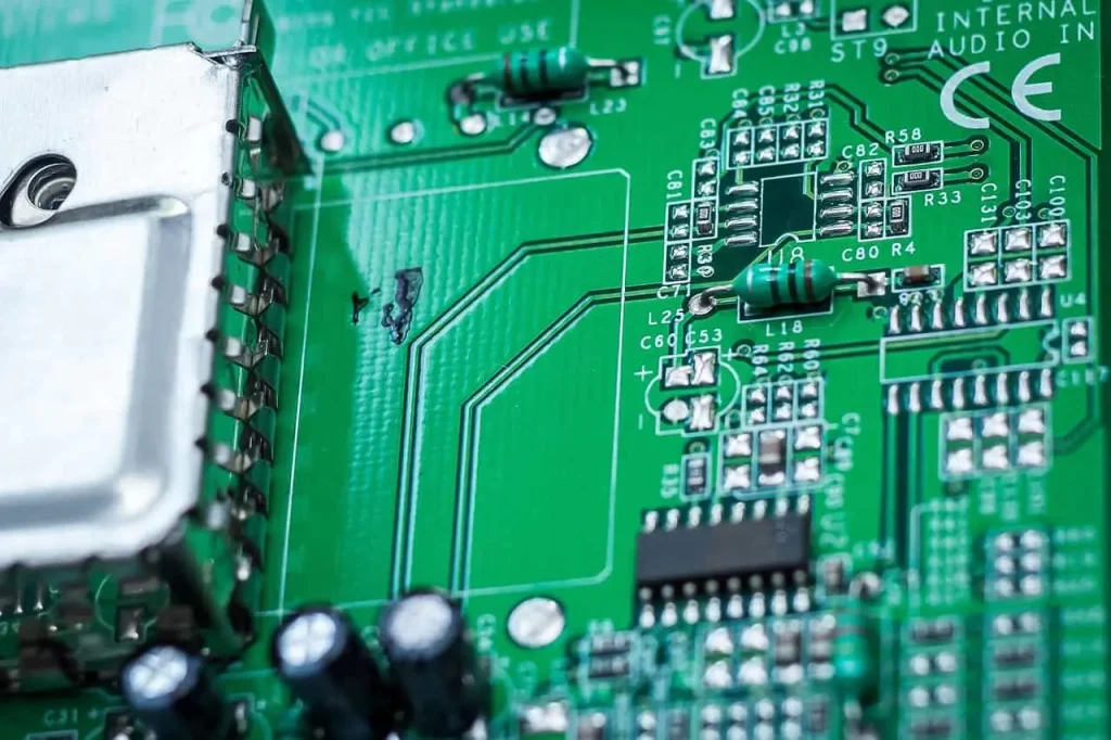
HDI (High-Density Interconnect) PCBs are a crucial technology in modern electronic products, widely used in smartphones, communication devices, and high-performance computing systems. Compared to traditional PCBs, HDI boards have higher wiring density, smaller via diameters, and more complex layer stack-up structures, enabling them to achieve more functions within a limited space. However, precisely because of their intricate structure and complex processes, HDI PCB manufacturing faces numerous technical challenges.
From design to production, HDI PCBs require multiple high-precision processes, such as laser drilling, micro-blind via plating, and fine circuit fabrication. Deviations in any step can affect the performance and reliability of the final product. Therefore, HDI PCB manufacturing not only tests equipment capabilities but also process control levels. Companies like Topray Circuits, by integrating design, manufacturing, and testing resources, can effectively address these complex challenges and achieve high-quality delivery.
Key Challenges in HDI Manufacturing
• High Difficulty in Micro-Blind Via Machining
HDI PCBs extensively use micro-blind vias, which are typically very small in diameter and require laser drilling, demanding extremely high equipment precision.
• Electroplation Uniformity Control
Electroplating on the inner walls of micro-orifices must be uniform; otherwise, poor conductivity or reliability issues can easily occur.
• Fine Circuit Fabrication
HDI boards have extremely small linewidths and spacings, requiring strict control over exposure and etching processes. Even slight deviations can cause short circuits or open circuits.
• Interlayer Alignment Accuracy
When stacking multiple layers, alignment errors must be controlled within a very small range; otherwise, connection reliability will be affected.
• High Material Stability Requirements
HDI boards often use high-performance materials, and the stability of these materials under high temperature and pressure directly affects the quality of the finished product.
· Complex Multi-Lamination Process
HDI typically involves multiple lamination processes, resulting in a long process flow and high control difficulty.
· Comparison of Manufacturing Challenges between HDI and Traditional PCBs
Compared to traditional PCBs, HDI PCBs present significantly increased manufacturing challenges. Traditional PCBs mainly rely on mechanical drilling and conventional circuit processing, which are mature and relatively inexpensive; while HDI PCBs require laser drilling and high-precision imaging technology, resulting in higher equipment investment. While conventional multilayer boards also feature multilayer designs, their interlayer connections are relatively simple. HDI (High-Density Interconnect) boards, however, employ blind vias, buried vias, and even arbitrary layer interconnects, resulting in a much more complex structure. Furthermore, HDI boards have a significantly higher circuit density than traditional PCBs, meaning that even minute errors are amplified, impacting overall performance. Therefore, from a manufacturing perspective, HDI is not only a technological upgrade but also a comprehensive test of the entire production system’s capabilities.
Frequently Asked Questions (FAQs)
Q: Why does HDI use laser drilling?
A: Because mechanical drilling cannot achieve such small hole diameters and high precision requirements.
Q: Why are micro-blind vias prone to problems?
A: The small hole diameter and high plating difficulty can easily lead to uneven filling or voids.
Q: Why are HDI boards expensive?
A: Complex processes, expensive equipment, and difficulty in controlling yield.
Q: What are the effects of interlayer alignment errors?
A: They can lead to electrical connection failures or signal instability.
Practical Application Examples
For example, in smartphone motherboards, HDI PCBs need to accommodate a large number of chips and signal lines within a very small space. This necessitates a large number and dense distribution of micro-blind vias. Uneven electroplating can lead to signal transmission abnormalities. In high-end communication equipment, HDI boards not only require high density but also excellent signal integrity, placing higher demands on material selection and manufacturing precision. In these high-standard applications, specialized manufacturers like Topray Circuits can solve challenges in micro-via processing, electroplating control, and multilayer lamination through advanced equipment and mature processes, thereby ensuring stable product performance.
From laser drilling to electroplating and multilayer lamination, every step in the HDI PCB manufacturing process requires precise coordination. Errors at any stage will accumulate and amplify. Furthermore, the production environment, equipment stability, and subtle adjustments to process parameters also significantly impact the final quality. HDI PCB manufacturing is a highly systematic engineering project requiring a deep integration of technology, equipment, and experience. Companies must not only possess advanced manufacturing capabilities but also a comprehensive quality control system. Manufacturers like Topray Circuits, which provide one-stop services, can participate in optimization from the early stages of design, reducing manufacturing difficulties from the source, while strictly controlling quality during the production and testing phases, thereby ensuring that HDI PCBs remain stable and reliable in high-density, high-performance applications.