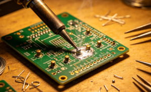
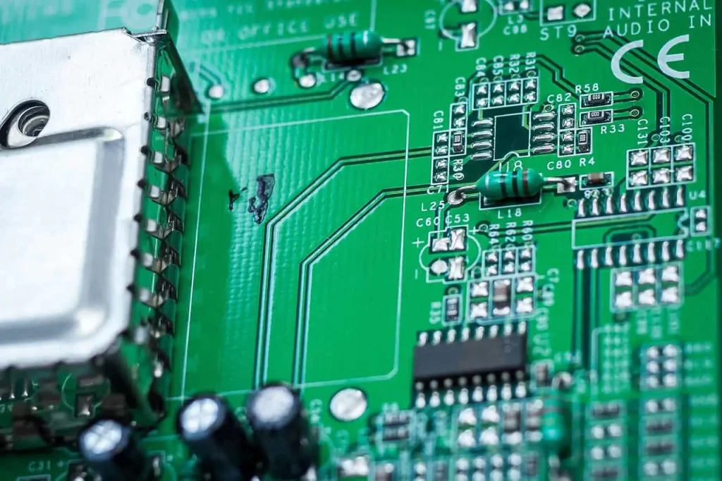
In modern high-speed electronic design, PCB routing is no longer simply about “connecting lines.” As signal frequencies continue to increase, signal integrity becomes a critical factor affecting product performance, stability, and even success or failure. Simply put, signal integrity refers to whether a signal maintains its original waveform and timing characteristics during transmission. Improper routing can lead to problems such as reflections, crosstalk, and delay mismatches, resulting in system errors, functional abnormalities, or even complete failure. Meanwhile, as the industry’s demand for high-density, high-reliability products increases, professional manufacturers like Topray Circuits, providing one-stop services from PCB layout to manufacturing and testing, are helping companies achieve high-quality design goals more efficiently. Good routing relies not only on design experience but also on manufacturing processes and overall solutions.
Wiring Method for Enhancing Signal Integrity
· Control Impedance Matching
High-speed signals must ensure continuous impedance of transmission lines; otherwise, reflections are likely to occur. A common practice is to use microstrip or stripline structures and calculate the impedance based on the dielectric parameters.
· Shorten the Signal Path
The shorter the signal path, the less loss and interference. Critical high-speed signals should be routed in straight lines as much as possible, minimizing unnecessary bends and vias.
· Utilize Ground Planes Effectively
A complete ground plane provides a stable reference path, reducing return path uncertainty and thus lowering noise and EMI issues.
· Reduce Crosstalk
Maintain spacing between high-speed signals, adhering to the “3W rule” (spacing ≥ 3 times trace width) to effectively reduce coupling between adjacent signals.
· Control Vias Number
Vias introduce parasitic inductance and capacitance, affecting signal quality. Vias should be used sparingly on critical lines.
· Symmetrical Differential Signal Routing
Differential pairs must have matched lengths and consistent spacing to avoid imbalances that increase common-mode noise.
Comparison of effects of different wiring methods
In PCB design, different routing strategies directly impact signal quality. For example, while simple single-ended routing is prone to interference in high-speed environments, differential routing effectively suppresses noise and improves anti-interference capabilities. Furthermore, while arbitrary routing saves time, it introduces impedance discontinuities; in contrast, precisely calculated impedance-controlled routing, although more complex, significantly improves system stability. Furthermore, the design differences between having a ground plane and not having one are significant: the former provides a stable return path and a cleaner signal; the latter is prone to loop noise.
Frequently Asked Questions
Q: Why is impedance control essential for high-speed signals?
A: Because impedance discontinuities can cause signal reflections, affecting waveform integrity.
Q: Do vias really affect signals?
A: Yes. Vias introduce parasitic parameters, with a particularly noticeable impact at high frequencies.
Q: Are more ground lines always better?
A: Not necessarily more, but rather forming a complete and continuous ground plane.
Q: Must differential lines be of equal length?
A: Yes, otherwise timing discrepancies will occur, degrading signal quality.
Practical Examples
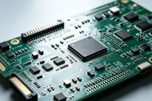
For example, when designing a high-speed communication board, improper USB 3.0 or DDR signal routing can easily lead to data errors. Engineers typically use differential routing and strictly control length errors within specified limits. Simultaneously, a complete ground plane design ensures the shortest possible signal return path. In RF circuit design, excessive bends in traces can lead to impedance abrupt changes, affecting signal transmission efficiency. Therefore, many high-end projects leverage professional service providers like Topray Circuits, utilizing their HDI or RF PCB technologies to achieve more precise routing and manufacturing, ensuring stable product performance.
Many issues in PCB design often arise from details, such as whether to use 45° instead of 90° corners, whether power and signal layers are layered, and whether critical lines are kept away from noise sources. These seemingly minor optimizations can have a cumulative impact on the final signal integrity. From impedance control to layer stack-up, from routing rules to manufacturing processes, every step is crucial.
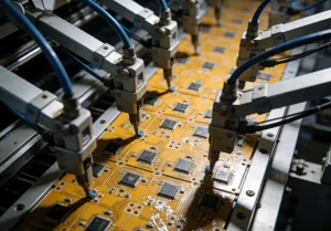
In actual projects, design experience alone is often insufficient; comprehensive optimization in conjunction with manufacturing and testing is also necessary. Service providers like Topray Circuits, with complete supply chain capabilities, can control quality throughout the entire process from PCB layout and manufacturing to assembly and verification, offering a significant advantage, especially for high-frequency, high-speed, and high-reliability products. This one-stop service not only shortens the development cycle but also effectively reduces errors between design and production. Improving signal integrity is not a breakthrough in a single technology, but rather the result of the synergistic effect of design specifications, wiring techniques, and manufacturing capabilities. Only by adhering to standards and meticulousness in every step can we ensure that the signal remains stable throughout the entire transmission process, thereby allowing the product to perform reliably in complex application environments.