


Tel :+86 13425156463
Email:sales@toplinecircuit.com
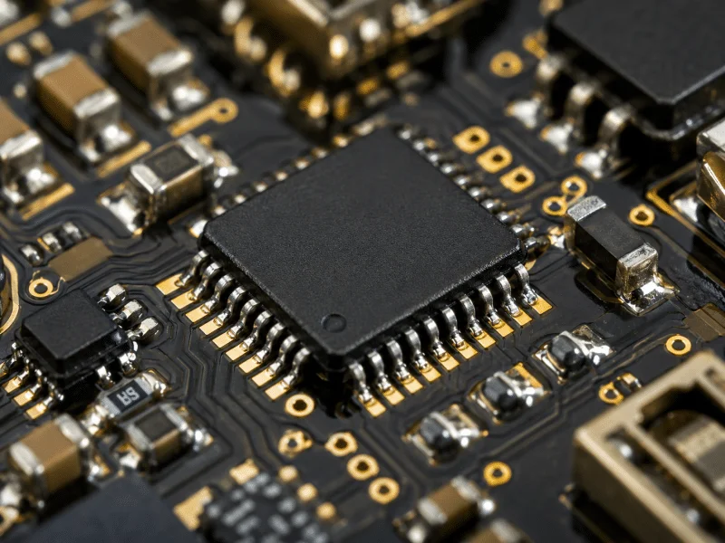
PCBA manufacturer evaluation detail with fine-pitch SMT components and clean solder joints

How to Choose the Right PCBA Manufacturer for BOM Review, Testing, and Production Risk

Choosing a PCBA manufacturer is not only a price decision. A low quotation may look useful at first. It may
09/07/2026
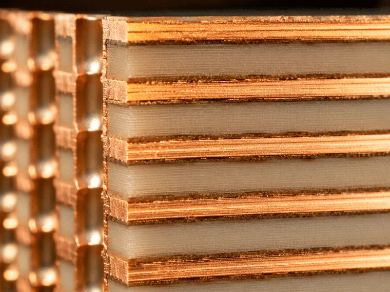
High-frequency PCB material cross-section showing controlled dielectric substrate layers and copper interface for RF signal stability.

Controlled Impedance vs Controlled Dielectric

High-speed digital and radio frequency (RF) designs require precise signal management to prevent data corruption and ensure system reliability. Hardware
04/07/2026
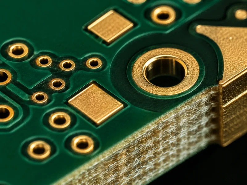
Bare multilayer PCB detail showing ENIG gold pads and microvias for fabrication and stack-up verification before assembly.

What Files Are Required for an Accurate PCB Assembly Quotation?

Requesting a PCB Assembly quote is often the first formal step in moving a hardware project from design to production.
04/07/2026
Flex PCB assembly detail showing surface mount components and local stiffener area on polyimide circuit for manufacturing risk review.

Flex PCB Assembly Risks Buyers Should Verify Before Mass Production

Flexible circuits offer significant advantages for compact electronic designs, wearable devices, and dynamic moving applications. However, the transition from a
02/07/2026
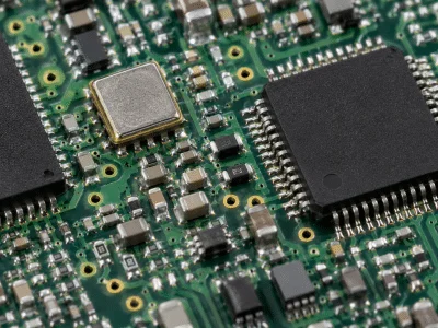
PCBA assembly detail showing fine-pitch SMT components and ENIG pads for turnkey and consigned project evaluation

Difference Between Turnkey and Consigned PCB Assembly and How to Choose

When preparing for PCB production, hardware teams must decide who will handle component procurement. This decision defines the assembly model
30/06/2026
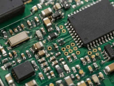
PCBA assembly detail showing fine-pitch SMT components and ENIG pads for quality evaluation

How to Evaluate a PCB Assembly Supplier Before Production

Choosing the right PCB assembly supplier is one of the most critical decisions in hardware development. A low quotation does
30/06/2026
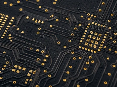
High frequency PCB material detail with fine RF routing, plated vias, ENIG pads, and laminate edge texture

High Frequency PCB Material Selection Risks Before Production

High frequency PCB material selection is not only about choosing a low-loss laminate. The material must also match the signal
28/06/2026
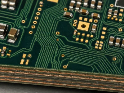
Multilayer PCB stack-up detail with laminated board edge, controlled routing traces, plated vias, and ENIG pads

Multilayer PCB Stack-Up Design Issues That Affect Controlled Impedance

Controlled impedance is not created by trace width alone. In a multilayer PCB, the stack-up determines how signal layers, reference
25/06/2026
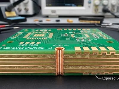
FR4 PCB material detail with green solder mask, plated vias, ENIG pads, and exposed multilayer edge structure Featured Image Export Requirement:

What Is FR4 PCB Material and How to Choose the Right Grade

FR4 is often treated as a standard PCB material choice. That is reasonable for many general electronic products, but it
25/06/2026
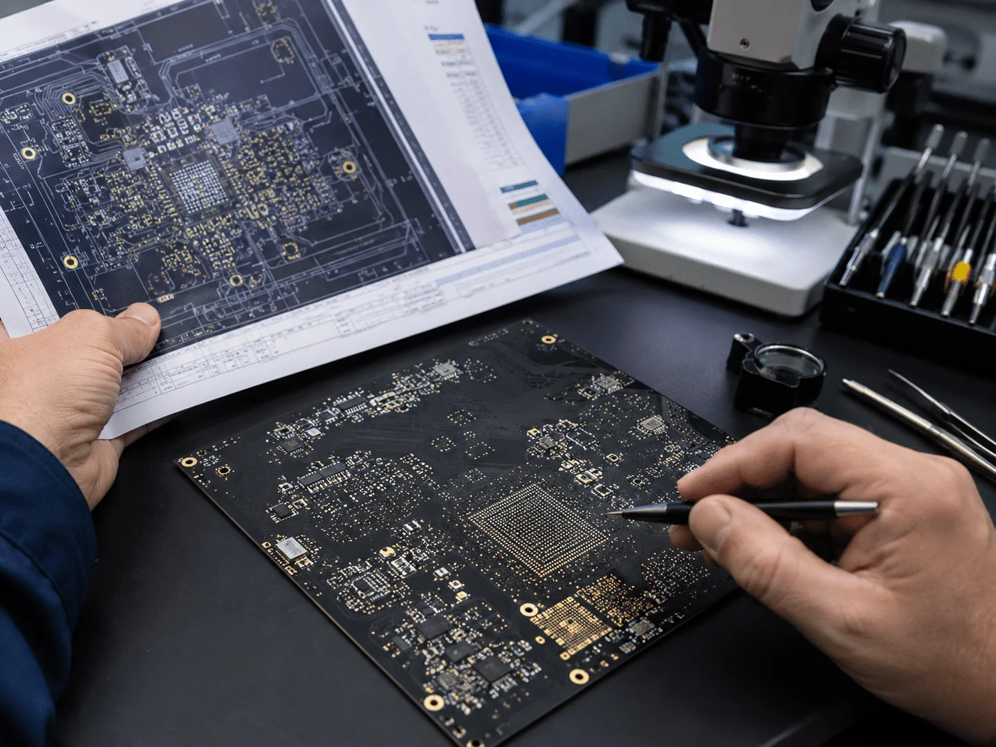
Engineer reviewing an HDI PCB stack-up and microvia design before manufacturing

How to Evaluate an HDI PCB Manufacturer Before Production

HDI PCB projects are not easy to judge from a quotation alone. A board may look simple in the Gerber

19/06/2026
GET A FREE QUOTE