

PCB Design Input Checklist: What to Send Before Layout Starts
Before PCB layout starts, send the schematic, verified BOM, component data, board outline, and the constraints that control placement and routing. A revision also needs
 Skip to content

Home / PCB Design & Engineering / How to Choose the Right PCB Layer Count for Your Design
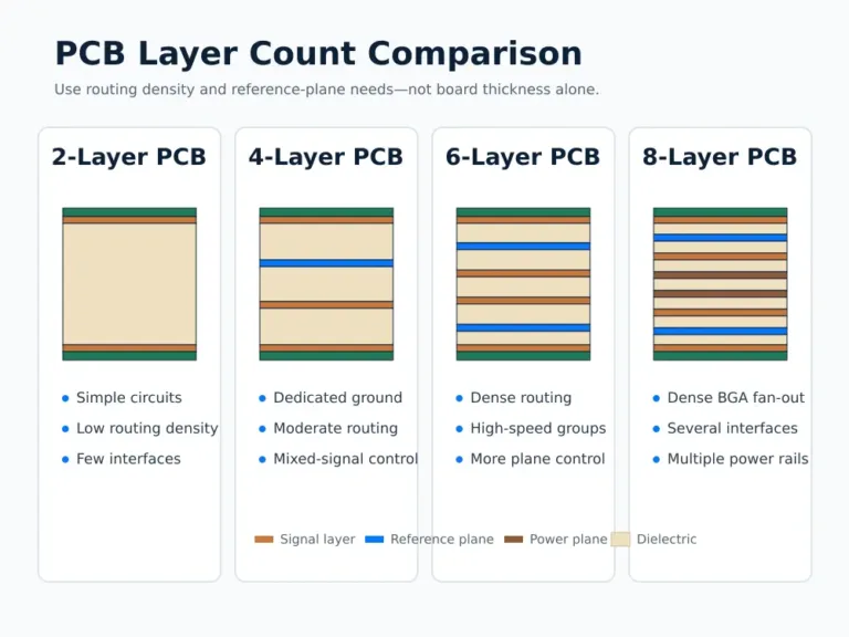
A PCB needs enough layers to route signals, provide stable reference paths, distribute power, and fit the required board size. Too few layers can force long traces, split return paths, and crowded fan-out. Too many layers add fabrication steps and may raise cost without solving a real problem.
The right PCB layer count comes from the circuit, component packages, layout density, signal requirements, and stack-up plan. Choose the layer count before detailed routing, then confirm the stack-up with the PCB manufacturer.
Do not begin with a fixed answer such as four or six layers. Begin with the board requirements. List the signals, power rails, large packages, connectors, controlled impedance nets, and mechanical limits. This creates a layer budget before routing starts.
The board area also matters. A large board may route on fewer layers because traces have more space. A compact board with the same circuit may need more signal layers. Component placement can change the answer as much as the schematic does.
Ask these questions first:
How many signal groups must cross the board?
Does the design use a dense BGA, FPGA, processor, or fine-pitch connector?
Which signals need controlled impedance or a continuous reference plane?
How many power rails need wide copper areas or dedicated planes?
Can the board size grow, or is the mechanical outline fixed?
Are there EMI, crosstalk, thermal, or isolation concerns?
Layer count rises when the design needs more routing space or more reference planes. A high-pin-count package is a common driver. The inner rows of a BGA need escape paths, and each routing channel uses space. Large numbers of power and ground pins can reduce the signal-routing demand, so the package must be reviewed instead of judged only by pin count.
| Design factor | Why it affects layer count | What to check |
| Routing density | More nets need more routing channels. | Placement, board area, via use, and trace rules |
| BGA or fine-pitch escape | Inner pins may need extra signal layers or HDI routing. | Pitch, pad size, via type, and breakout plan |
| High-speed signals | Signals need clear reference planes and controlled geometry. | Interface groups, impedance targets, and return paths |
| Power distribution | Multiple rails need enough copper area and low-impedance paths. | Current, rail count, plane or pour strategy, and decoupling |
| EMI and crosstalk | Poor layer pairing can increase field spread and coupling. | Signal-to-reference spacing and plane continuity |
| Mechanical outline | A smaller board leaves less space for traces and fan-out. | Fixed dimensions, connectors, mounting holes, and keep-outs |
Do not count only signal layers. Ground and power planes are part of the total stack-up. A six-layer board may provide only three or four practical routing layers, depending on how the reference and power layers are assigned.
A two-layer PCB can suit a simple circuit with low routing density. It works better when the board has enough area and few sensitive signal groups. The layout still needs a clear return path. A ground pour does not help if narrow gaps and routing cuts break the current path.
A two-layer option becomes harder to defend when high-speed interfaces cross the board, the component pitch is tight, or the design needs several clean power regions. The issue is not only whether every net can connect. The finished routing must also preserve reference continuity and spacing.
Use two layers when the layout stays simple after placement. Move to a multilayer stack-up when routing depends on narrow channels, long detours, or broken ground areas.
Four layers give the designer more control over signal references and power routing. A common plan uses outer layers for components and routing, plus inner layers for ground and power distribution. That arrangement is not correct for every design. Some boards benefit from two ground references and routed power instead of a full power plane.
The key question is whether each important signal has a nearby and continuous reference. A solid ground plane can provide a lower-impedance return path. It can also make controlled impedance easier to define because trace geometry relates to a known reference layer.
Choose four layers when a two-layer layout becomes crowded, return paths are hard to protect, or controlled impedance needs a defined stack-up. Confirm the dielectric spacing and trace geometry with the manufacturer before releasing the design.
When Six or Eight Layers Make More Sense
Six or eight layers become useful when the design needs more signal layers and more reference control at the same time. This often occurs with dense processors, FPGAs, memory buses, high-pin-count BGAs, several high-speed interfaces, or a compact mechanical outline.
Extra layers can separate signal groups. They can also place reference planes next to important routing layers. This can reduce layout compromises, but only when the layer order is planned. Adding layers without a routing purpose can create unused copper and unnecessary cost.
| Layer count | Typical fit | Main decision check |
| 2 layers | Simple circuits with low routing density and enough board area | Can routing preserve a useful ground return path? |
| 4 layers | Moderate density with clearer ground reference and power routing | Does the stack-up support the required reference and impedance geometry? |
| 6 layers | More routing channels, several signal groups, or denser packages | How many layers are signals, and which planes reference them? |
| 8+ layers | Dense BGA escape, multiple interfaces, power needs, or limited board area | Does each added layer have a defined routing, reference, or power purpose? |
These are decision ranges, not fixed rules. A simple but noise-sensitive board may need more layers. A larger board with complex logic may route on fewer layers if placement and package escape allow it.
A layer budget turns the selection into a repeatable engineering check. It also gives the PCB manufacturer better information for stack-up review.
Mark every interface that needs controlled impedance or a continuous reference plane.
Review the largest BGA or fine-pitch package and estimate its escape needs.
Estimate routing layers from net density, board area, placement, and design rules.
Reserve ground reference layers before assigning power and low-speed routing.
Decide which power rails need planes and which can use pours or wide traces.
Keep the stack-up reasonably balanced and confirm manufacturability with the fabricator.
Route the most constrained interfaces first, then check whether the layer budget still works.
The first estimate may change after placement. That is normal. Changing the layer count early is easier than forcing a weak layout after most routes are complete.
A board can be fully connected and still have a poor stack-up. These mistakes often appear when layer count is treated only as a routing problem.
Mistake 1: Minimize layers before checking risk. Choosing the fewest layers at any cost can break return paths and crowd fan-out. The saved fabrication cost may be offset by a larger board, harder routing, more EMI work, or another layout revision.
Mistake 2: Give every voltage its own plane. A dedicated power plane is not required for every rail. Some rails can use pours or wide traces. The choice depends on current, noise, placement, and available area.
Mistake 3: Add signal layers without reference planning. Signals on adjacent layers can couple if their routing and references are not planned. Layer order matters as much as the total number.
Mistake 4: Change the stack-up after routing. Changing layer count changes dielectric spacing and trace geometry. Existing impedance rules may no longer be valid.
Mistake 5: Treat the prototype stack-up as temporary. The prototype and production board should use compatible stack-up assumptions. A late change can affect impedance, via structure, thickness, and assembly fit.
The manufacturer cannot confirm a useful stack-up from the layer count alone. Send enough design data to show the electrical and mechanical requirements.
Gerber or ODB++ data and drill files
Fabrication drawing with finished thickness and copper requirements
Proposed layer order and layer names
Controlled impedance targets and the affected nets
Material requirements or approved alternatives
Via types, BGA pitch, and any HDI structure notes
Board outline, keep-outs, and mechanical limits
Current or thermal requirements when they affect copper allocation
The exact stack-up depends on material availability, dielectric thickness, copper weight, impedance targets, via structure, and production requirements. These items should be confirmed during DFM review.
Is a four-layer PCB always better than a two-layer PCB? No. Four layers often make reference-plane planning easier, but a simple two-layer design may be enough. The circuit, board area, and routing quality decide the answer.
Do more PCB layers always reduce EMI? Not by itself. More layers help only when signals, reference planes, and power distribution are assigned correctly. A poor eight-layer stack-up can still create EMI problems.
How many layers does a BGA board need? There is no fixed answer. Check ball pitch, row depth, pad and via rules, unused pins, and the number of power and ground balls. Build a breakout plan before fixing the layer count.
Does every multilayer PCB need a dedicated power plane? No. Some designs use routed power or copper pours. The decision depends on current demand, rail count, noise sensitivity, and available layer area.
Can I change the layer count after routing? Yes, but the change may affect impedance, trace width, via structure, finished thickness, and cost. Recheck the stack-up and routing rules before release.
Why are even PCB layer counts more common? Even layer counts often support a more symmetric construction and are common in manufacturing. Odd counts may be possible, but the fabricator should review the structure before layout release.
Choose the lowest layer count that still supports clear routing, continuous return paths, power distribution, mechanical limits, and the required stack-up. Do not choose from cost alone. A layer must have a defined job as a signal, reference, or power layer.
Topline Circuit can review the proposed stack-up, Gerber data, fabrication drawing, impedance targets, and project requirements. Use the Contact page to send the project files for engineering review and quotation support.
Our team can help you evaluate the board structure, materials, component assembly, and testing requirements based on your product’s operating environment and performance needs.

Before PCB layout starts, send the schematic, verified BOM, component data, board outline, and the constraints that control placement and routing. A revision also needs

Component sourcing can account for a large part of a turnkey PCB assembly quotation. The cost depends on the exact parts, available stock, purchasing channels,
Controlled dielectric specifies the material and spacing in a PCB stack-up. Controlled impedance specifies an electrical target for selected traces. A board may need one
A PCB needs enough layers to route signals, provide stable reference paths, distribute power, and fit the required board size. Too few layers can force