

PCB Design Input Checklist: What to Send Before Layout Starts
Before PCB layout starts, send the schematic, verified BOM, component data, board outline, and the constraints that control placement and routing. A revision also needs
 Skip to content

Home / Industry Applications / Controlled Dielectric vs. Controlled Impedance: What Should You Specify?
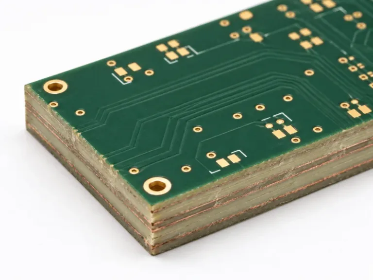
Controlled dielectric specifies the material and spacing in a PCB stack-up. Controlled impedance specifies an electrical target for selected traces. A board may need one requirement or both, depending on what the design must achieve.
A controlled dielectric specification defines part of the PCB’s physical construction. It usually identifies the insulating material between copper layers and the required finished thickness.
For example, an engineer may calculate a trace’s impedance using a defined distance to its reference plane. The manufacturer then builds the board to that agreed layer spacing.
The drawing must identify which spacing is controlled. A note that says only “controlled dielectric” does not tell the manufacturer which layers matter or what thickness variation is allowed.
A useful note identifies the signal layer, reference plane, dielectric material, finished thickness, and tolerance. It should also say whether the manufacturer may substitute another material.
That substitution rule matters when the design relies on material properties. A different material can change the assumptions used in the engineer’s calculation.
Controlled dielectric gives the designer defined stack-up inputs. It does not, by itself, make finished trace impedance an acceptance requirement.
Controlled impedance sets an electrical target for identified traces. The drawing should give the target value, tolerance, routing layer, and trace identification.
It should also say whether the requirement applies to a single-ended trace or a differential pair. For a pair, the trace spacing is part of the geometry the manufacturer needs to review.
The manufacturer checks whether the target is achievable with the proposed stack-up and finished trace geometry. That review may produce a proposed change to material, layer spacing, trace width, or pair spacing.
The designer should review any change that affects the approved layout. The purchase documents should also say whether a calculation, coupon measurement, or report is required.
“Controlled impedance” alone is not a complete fabrication note. It does not identify which traces need control or what measured result would pass.
Even “50 Ω controlled impedance” needs more detail. The manufacturer needs the relevant layer, reference plane, trace geometry, and acceptable tolerance.
Controlled dielectric defines whether the board follows a specified stack-up. Controlled impedance defines whether selected traces meet an electrical target.
Dielectric material and thickness affect impedance, but they are only part of the PCB stack-up. Trace width, copper geometry, reference planes, and differential-pair spacing also matter.
Consider two traces on the same layer above the same reference plane. They use the same dielectric material and thickness. If their widths differ, their impedances will generally differ.
Both traces could be on a board that meets the controlled dielectric requirement. That does not mean both traces meet the same impedance target.
A manufacturer may also propose different stack-ups that meet one impedance target. If your design requires a specific material or layer spacing, state that requirement separately.
The choice depends on what you need to accept: the specified stack-up, the impedance result, or both.
Controlled dielectric can suit a design that has already been modeled around a defined stack-up. The engineering team calculates the expected impedance from its material, spacing, and trace geometry.
Check that the drawing states the finished dielectric thickness required. The value used during an early design estimate may not match the construction proposed for production.
Check the material properties used in the electrical model as well. The proposed material and construction should match the assumptions behind that model.
If a specified material is unavailable, ask the manufacturer for a revised stack-up. The engineer can then assess its thickness and properties before approving a substitution.
Controlled dielectric may also matter when layer spacing serves another design requirement. Overall board thickness or another structure may limit what the manufacturer can change.
If selected traces must meet a finished impedance tolerance, add that requirement explicitly. A controlled dielectric note does not identify those traces or define how their impedance will be checked.
Use controlled impedance when selected traces must meet an electrical target. First, identify those traces by net name, net class, or another clear reference.
State the target and tolerance for each distinct structure. Include the signal layer, reference plane, and whether the structure is single-ended or differential.
Give the nominal trace width shown in the artwork. For a differential pair, give the nominal width and spacing of the two traces.
Ask the manufacturer to review the production stack-up before fabrication. If it differs from the design stack-up, the engineer should assess the proposed material and geometry.
Decide what evidence the order requires. A calculation predicts the result for a proposed build. A coupon measurement checks a representative fabricated structure.
If you need a coupon measurement and report, request them in the fabrication documents. Do not assume that the phrase “controlled impedance” defines the same deliverables for every order.
Specify both when the stack-up has fixed requirements and selected traces must meet impedance targets.
For example, a design may require a particular material and layer separation. The same board may also contain traces with defined impedance limits.
The manufacturer must check whether the target is achievable within those limits. If the requirements conflict, the engineer needs to resolve the conflict before production.
Mark which material and thickness values cannot change. Then identify any trace widths or pair spacings the manufacturer may propose to adjust.
Avoid fixing every dimension without checking feasibility. A fixed material, dielectric thickness, trace width, pair spacing, and impedance target may leave no practical adjustment available.
Ask the manufacturer to report that conflict clearly. The approved fabrication package should record the final construction and electrical requirements.
The drawing must connect each impedance target to a real trace structure. A short list in the fabrication notes can identify the controlled nets, layers, targets, and tolerances.
Provide the stack-up with the same drawing revision. It should show the layer order and dielectric construction relevant to the controlled traces.
For each structure, check that the files answer these questions:
The Gerber files must match the drawing under review. An impedance target from one revision should not be paired with artwork from another.
Also distinguish an early stack-up estimate from an approved production stack-up. Review the manufacturer’s proposal against the actual routed board before release.
Start with the stack-up used in the design. Compare its dielectric material and thickness with the manufacturer’s proposed build.
Then review the finished copper construction and any proposed trace-width or pair-spacing change. Check every controlled layer affected by the proposal.
A change can affect more than impedance. A narrower trace may conflict with another design requirement. A different dielectric thickness may change overall board thickness.
Ask the manufacturer to mark revisions clearly. An updated stack-up or drawing is easier to review than a list of changed numbers in an email.
Keep the approved version with the order. This is particularly useful when the prototype and production boards are made under separate purchase orders.
If the fixed construction and impedance target cannot both be met, the design team must decide what may change. Record that decision in the approved fabrication files.
Controlled dielectric is checked against the agreed construction. The order should define the relevant material and finished dimensional requirements.
Controlled impedance may first be reviewed through a calculation. That calculation predicts the result using the proposed material and trace geometry.
When measured verification is required, a test coupon can represent an agreed structure. Confirm which layer, geometry, and target each coupon covers.
A coupon does not measure every routed trace on every board. Its result should be interpreted within the scope agreed before production.
The calculation and measurement answer different questions. If the proposed material or geometry changes, the calculation may need updating.
Agree on the acceptance limits and report contents before ordering. This makes it possible to match a reported result to the structure specified in the drawing.
Does controlled dielectric guarantee a 50 Ω trace?
No. Dielectric material and thickness are only part of the structure. Specify the applicable traces and impedance tolerance if 50 Ω is required.
Can another laminate be used for a controlled-impedance board?
Only if your material rules permit it. Review the substitute material with the revised stack-up and impedance calculation.
Is differential impedance always twice single-ended impedance?
No. The spacing between paired traces affects their coupling. Specify and review the differential target directly.
Does a test coupon measure every controlled trace?
No. It represents an agreed structure. Confirm which layers and geometries the coupon covers.
Can the manufacturer change a trace width to meet impedance?
Only within the agreed change process. Mark fixed widths clearly and review proposed artwork changes before production.
Before releasing the board, decide whether acceptance depends on the stack-up, the impedance result, or both. Put those requirements in the same drawing revision and resolve proposed changes before fabrication.
Our team can help you evaluate the board structure, materials, component assembly, and testing requirements based on your product’s operating environment and performance needs.

Before PCB layout starts, send the schematic, verified BOM, component data, board outline, and the constraints that control placement and routing. A revision also needs
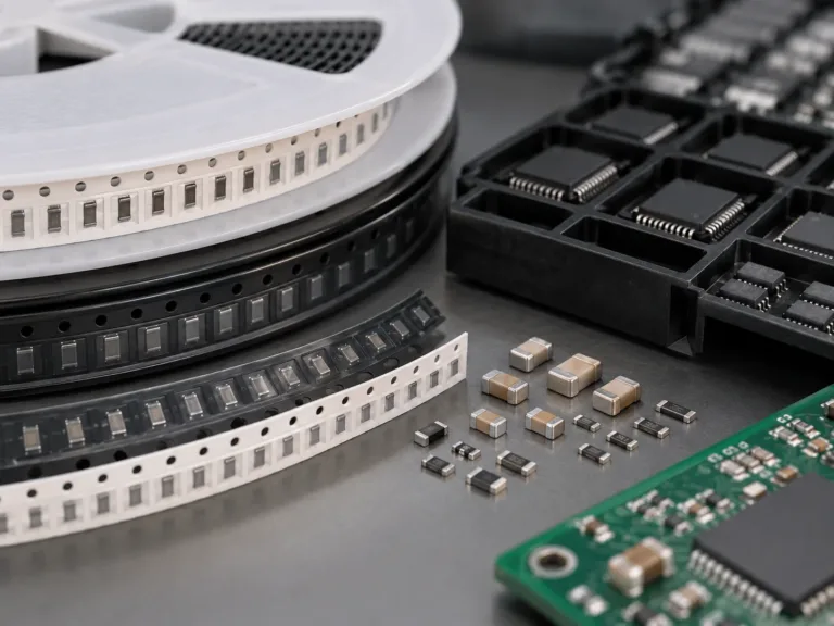
Component sourcing can account for a large part of a turnkey PCB assembly quotation. The cost depends on the exact parts, available stock, purchasing channels,
Controlled dielectric specifies the material and spacing in a PCB stack-up. Controlled impedance specifies an electrical target for selected traces. A board may need one
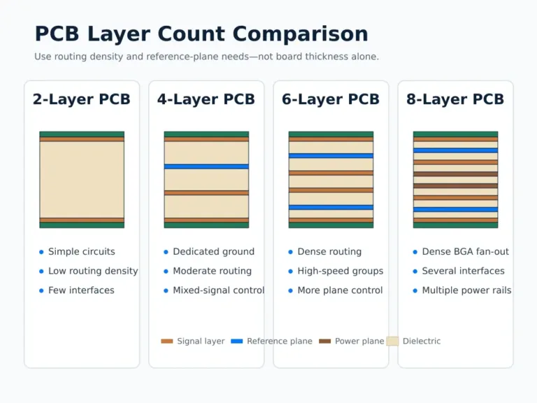
A PCB needs enough layers to route signals, provide stable reference paths, distribute power, and fit the required board size. Too few layers can force