


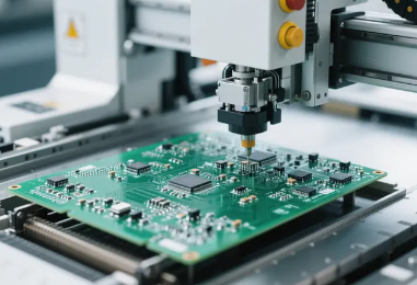
With the full-scale adoption of 5G technology, intelligent terminal devices are rapidly evolving toward being lighter, faster, and more highly integrated. Whether it is 5G smartphones, tablet computers, or wearable devices such as smartwatches, their core performance heavily depends on PCB (Printed Circuit Board) support. PCBs not only affect signal transmission speed, but also directly determine overall device stability, power consumption control, and space utilization efficiency. Therefore, selecting the appropriate PCB solution for different terminal devices has become a critical step in product design. This article systematically analyzes PCB selection strategies for 5G terminals from three perspectives: structure, materials, and application.
PCB Selection Solutions for 5G Smartphones
In smartphone designs that require both high performance and ultra-thin form factors, PCB selection must balance high-speed signal transmission and space constraints.
HDI High-Density Interconnect Board Solution
Due to extremely limited internal space, HDI boards have become the mainstream choice.
- Uses microvia structures to achieve multi-layer high-density routing
- Improves signal integrity and reduces crosstalk and delay
- Supports highly integrated layouts for SoC chips and RF modules
High-Speed Signal Material Selection
Materials directly impact 5G RF and high-speed data transmission performance.
- Low dielectric constant materials reduce signal delay
- Low-loss materials improve millimeter-wave transmission efficiency
- High-stability materials ensure long-term reliable operation
Functional Partition Design Optimization
Proper partitioning improves overall device stability.
- Physical isolation between RF and digital sections
- Centralized power section layout to reduce noise
- Optimized thermal paths in heat-generating areas
PCB Design Solutions for 5G Tablet Computers
Tablet devices require higher performance and better heat dissipation, demanding a balance between area and performance.
Multi-Layer Hybrid PCB Structure
Balancing performance and scalability is key in tablet design.
- 8–12 layer structures support complex circuits
- Separation of signal and power layers reduces interference
- Enhances stable power delivery for large-screen devices
High-Performance Material Configuration
Material selection directly affects long-term operation.
- Medium-low Dk materials improve response speed
- Low Df materials reduce high-speed transmission loss
- High Tg materials enhance heat resistance
Thermal and Power Optimization Design
Long-time operation requires strong thermal management.
- Added thermal vias to improve heat diffusion
- Thickened copper layers for better heat dissipation
- Optimized chip layout for centralized cooling
PCB Selection Solutions for Wearable Devices
Wearable devices prioritize extreme miniaturization and low power consumption.
Flexible PCB (FPC) Application
Flexible structures are essential for wearables.
- Bendable design adapts to complex shapes
- Saves space and improves wearing comfort
- Supports irregular structural layouts
Ultra-Thin High-Density PCB Design
Achieving high integration within limited space.
- Ultra-thin substrates reduce overall weight
- Miniaturized routing increases integration level
- Supports integration of multiple sensor modules
Low Power Consumption Optimization
Extending battery life is a key objective.
- Optimized power paths reduce energy loss
- Use of low-power component layouts
- Reduction of unnecessary signal switching
Comparison Table of PCB Materials and Structures for 5G Devices
| Device Type | Recommended PCB Type | Core Features | Main Objective |
| Smartphone | HDI multilayer board | High density, high-speed signals | Ultimate performance & thinness |
| Tablet | Multilayer hybrid PCB | High power, high stability | Balance performance & heat dissipation |
| Wearables | FPC / ultra-thin PCB | Flexible, low power | Miniaturization & battery life |
Key Differences in PCB Design Across 5G Terminals
Performance vs Power Consumption Priorities
Different devices prioritize different goals.
- Smartphones focus on high-speed processing
- Wearables prioritize long battery life and stable connectivity
Structural Complexity Differences
PCB structural requirements vary significantly.
- Smartphones require complex multi-layer designs
- Tablets are intermediate between phones and PCs
- Wearables adopt highly simplified structures
Material Selection Differences
Application scenarios determine material priorities.
- Smartphones: high-speed, low-loss materials
- Tablets: heat-resistant and stable materials
- Wearables: flexible and lightweight materials
With the continuous advancement of 5G technology, smartphones, tablets, and wearable devices present entirely different requirements for PCB design. From high-density interconnect structures to flexible material applications, from high-speed signal optimization to low-power system design, every detail directly affects device performance and user experience. Only by selecting PCB solutions tailored to specific product forms can the full potential of 5G devices be realized, achieving an optimal balance between performance, power consumption, and structure. As intelligent terminals continue to evolve, PCB technology will keep advancing and remain a core driving force behind industry innovation.