 Skip to content

Controlled Impedance PCBs
What Is a Controlled Impedance PCB?
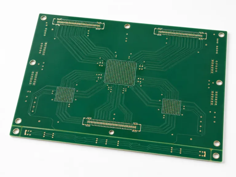
A controlled impedance PCB is manufactured so selected signal traces meet a defined electrical impedance. The target may apply to a single-ended trace, differential pair, microstrip, stripline, or another transmission structure.
The finished impedance depends on the complete PCB construction. Trace width, spacing, copper thickness, dielectric height, material Dk, reference planes, and solder mask must be reviewed together.
Types of Controlled Impedance PCBs
Single-ended impedance
A single signal trace is controlled relative to a reference plane. This structure is common in clock, RF, and other signal paths.
Differential impedance
Two coupled traces carry complementary signals. Their width, spacing, copper thickness, and reference plane must be controlled together.
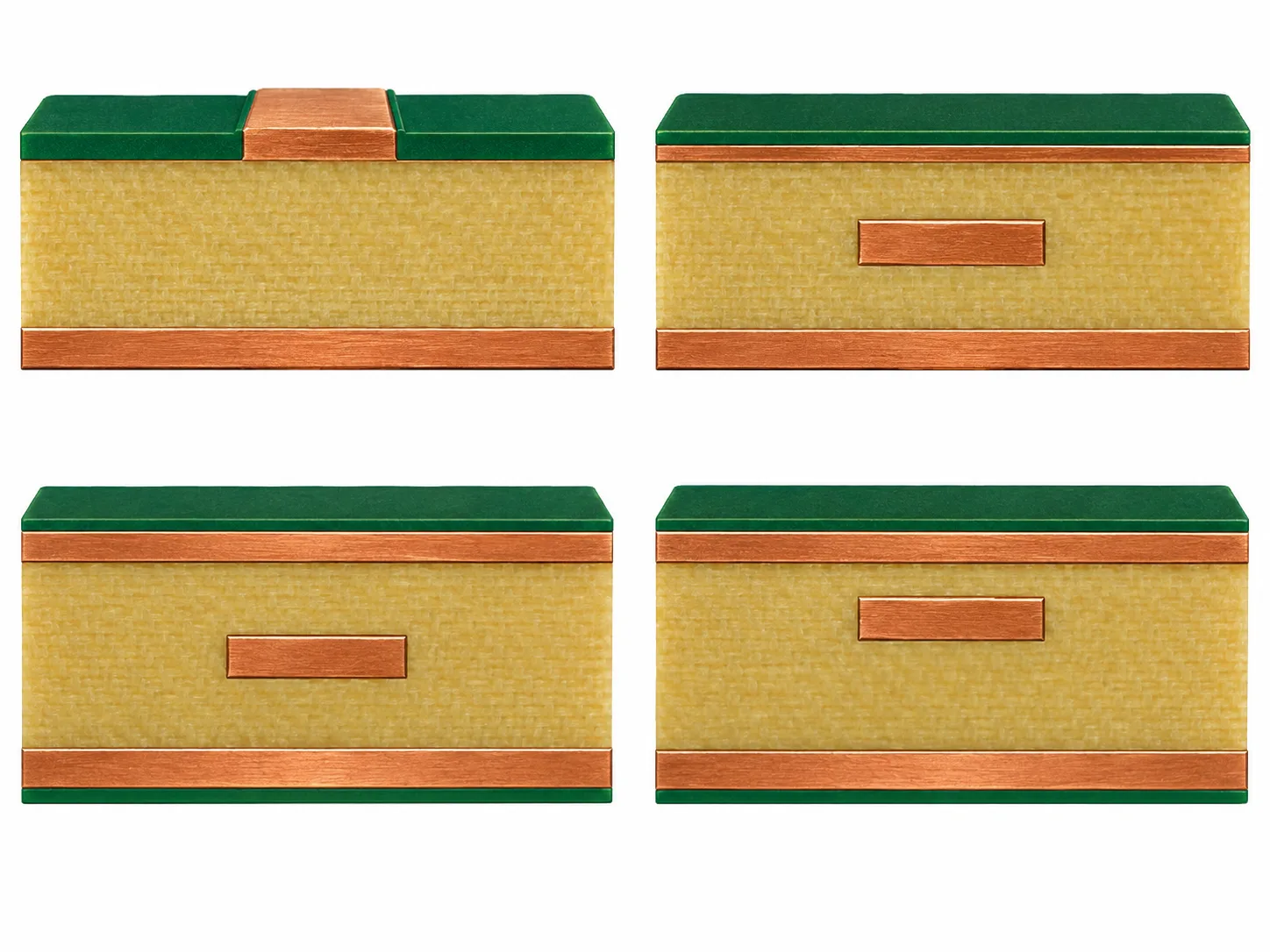
Microstrip and embedded microstrip
The signal trace is placed on or near an outer layer with one main reference plane.
Stripline
The signal trace is routed on an inner layer between reference planes for a more enclosed transmission structure.
Controlled Impedance PCB Applications
Controlled impedance is used when signal edge rate, data rate, or operating frequency makes the PCB trace behave as a transmission line.
The requirement may appear in standard FR-4 multilayer boards, HDI boards, flex and rigid-flex circuits, or low-loss RF constructions.
- Servers, AI hardware, and high-speed computing
- Ethernet and data communication equipment
- USB, HDMI, LVDS, PCIe, SATA, and DDR interfaces
- Telecom equipment and optical communication modules
- RF, microwave, antenna, and wireless systems
- Automotive sensing, cameras, and infotainment
- Industrial control and automation equipment
- Test, measurement, and data acquisition systems
Controlled Impedance PCB Capabilities
Topline Circuit supports controlled impedance requirements across different PCB structures. The final construction is reviewed against the supplied files and project specifications.
Single-Ended and Differential
Support for single-ended traces and differential pairs based on the target impedance, signal layer, and reference structure.
Transmission Structures
Microstrip, embedded microstrip, stripline, and coupled differential structures can be reviewed for manufacturability.
Stack-Up Review
Layer order, dielectric thickness, copper weight, reference planes, board thickness, and material selection are reviewed together.
PCB Constructions
Controlled impedance can be coordinated with multilayer, HDI, rigid, flex, rigid-flex, RF, microwave, and high-frequency PCB requirements.
Material and Geometry Review
Trace width, pair spacing, finished copper thickness, dielectric height, and material Dk are checked against the proposed construction.
Production Support
DFM review and engineering confirmation support the transition from prototype builds to repeat production.

Design Considerations for Controlled Impedance PCBs
Impedance requirements should be coordinated with the PCB manufacturer before the layout and stack-up are finalized. This helps prevent trace widths, spacing, or dielectric values from becoming difficult to manufacture.
- Confirm the stack-up before final routing
- Identify each controlled net, signal layer, and reference plane
- Allow for finished copper thickness and fabrication compensation
- Keep differential-pair width and spacing consistent
- Avoid unnecessary reference-plane gaps and return-path discontinuities
- Specify the target impedance, tolerance, and required verification scope