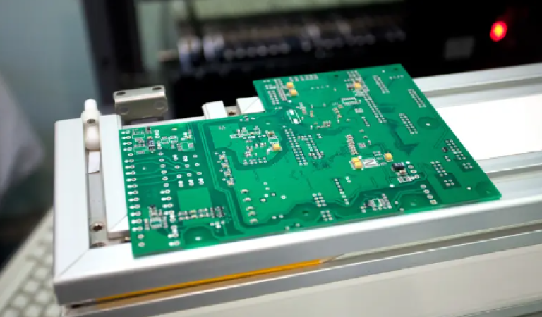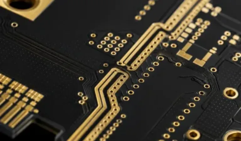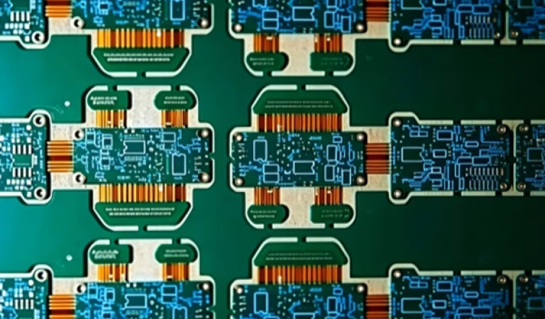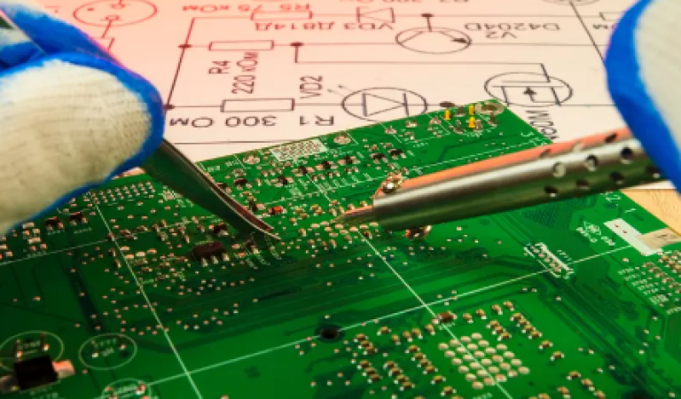


Prototype PCBs are used when a design needs to be checked before the project moves into a larger production stage. They allow engineering teams to verify board size, routing, component placement, electrical connections, and mechanical fit using a real fabricated board.
A prototype board is useful for new designs, revised circuits, replacement projects, and products that require a practical check before assembly. The purpose is not only to obtain a board sample. It is to identify design and manufacturing questions early, when changes are easier to manage.
New Product Development
A prototype PCB gives the design team a physical board for early validation. It can help confirm whether the layout, hole locations, connector positions, and component areas match the intended product structure.
Design Revisions Before Production
A revised PCB layout should be reviewed again before the next build. Changes to the stack-up, drill files, copper areas, or component locations can affect fabrication and assembly planning.
Projects Moving Toward PCBA
A bare prototype PCB can also support the next assembly stage. If the board will be assembled, pad design, solder mask openings, test access, and component spacing should be considered before fabrication.

What We Review Before Prototype PCB Manufacturing
A useful prototype PCB review starts with complete project data. Gerber files show the visible copper, solder mask, silkscreen, and outline layers. The manufacturer also needs drill data, fabrication notes, stack-up information when applicable, and any special material or impedance requirements.
Clear files help identify questions before fabrication begins. They also help avoid a situation where the physical sample does not match the intended design requirement.
| Review Area | What Buyers Should Confirm |
|---|---|
| Gerber files | Complete copper, solder mask, silkscreen, and outline data |
| Drill files | Hole types, slots, vias, and finished-hole notes |
| Board outline | Dimensions, cutouts, routes, and panel notes |
| Material notes | Thermal, electrical, or application requirements |
| Stack-up notes | Layer structure and dielectric requirements when needed |
| Fabrication drawing | Special instructions and acceptance criteria |
Gerber Files Must Match the Latest Revision
Gerber files should come from the final approved design revision. Older files, missing layers, or unclear version control can cause avoidable questions during engineering review.
Drill Data Needs Clear Notes
Drill files should define through holes, vias, slots, and other internal or mechanical features. If a hole type has a special purpose, that information should appear in the fabrication drawing or related notes.
DFM Review Supports Better Prototype Decisions
A DFM review can identify unclear fabrication notes, tight routing areas, unusual copper distribution, and assembly concerns before the board enters manufacturing planning. Use PCB design as the internal link when discussing Gerber review, DFM checks, and manufacturing file preparation.
Stack-Up and Material Planning
Prototype boards should use a stack-up and material approach that matches the project’s actual purpose. A simple circuit may not need detailed stack-up planning. A board with high-speed signals, multiple layers, dense routing, or special thermal requirements usually needs more engineering review.
Material selection affects board rigidity, thermal behavior, dielectric structure, copper adhesion, and later assembly conditions. The material should be reviewed with the application requirement instead of being selected only by a general name.
Multilayer and Dense Routing Projects
Projects with more routing layers, multiple power domains, or compact component areas may need a clearer stack-up plan. The layer arrangement should support routing, ground reference, and any signal-control needs.
For multilayer structures, link naturally to PCB manufacturing or the relevant Multilayer PCB product page once it is published.
High-Temperature Requirements
Products exposed to higher thermal stress may need a material review before fabrication. This can apply to boards with power devices, repeated thermal cycling, or demanding operating environments.
For thermal material considerations, use High Tg PCB as the related internal link.
High-Frequency Signal Requirements
RF, communication, and high-speed signal projects may need closer review of dielectric behavior, copper surface characteristics, routing geometry, and stack-up structure.
For relevant projects, use High Frequency PCB as the supporting internal link.
Prototype PCB Manufacturing Considerations
A prototype board should reflect the main design intent of the final project. It is not useful to simplify critical features only to make the first board easier to fabricate. Important routing, layer, material, and interface requirements should be reviewed before the prototype is released.
Controlled Impedance Must Be Identified Early
If the design includes controlled impedance traces, those requirements should be included in the project files. The target requirements need to match the final stack-up, trace geometry, copper thickness, and material construction.
For impedance-related routing and stack-up review, use Impedance Controlled PCBs as the internal link.
Dense Routing May Need an HDI Review
Fine-pitch components, compact BGA escape routing, microvias, or complex layer transitions may require an HDI structure rather than a standard prototype PCB build.
When the design includes these features, use HDI PCBs as the supporting product link. Do not link to a specific HDI application page unless the prototype project is clearly for that same application.
Copper Balance Should Not Be Ignored
Large copper-filled areas on one layer and light routing on another can affect lamination balance and board flatness. These areas should be visible in the Gerber files and included in the engineering review.
Preparing for Prototype PCB Assembly
Prototype PCB fabrication and assembly planning should be connected early. A bare board may be ready for fabrication but still create assembly problems if the component footprint, pad design, polarity marking, or test access is unclear.
If assembly is part of the project, provide the BOM, pick-and-place file, assembly drawing, and testing requirements together with the bare PCB files. This helps identify sourcing, placement, soldering, and inspection questions before the assembly stage.
| Assembly Item | What Buyers Should Prepare |
| BOM review | Manufacturer part numbers and approved alternatives |
| Placement data | Pick-and-place file and component location data |
| Assembly drawing | Polarity, connector, and special assembly notes |
| Test access | Test points and functional test requirements |
| Package concerns | BGA, QFN, or fine-pitch component notes |
BOM Review Helps Prevent Assembly Questions
A complete BOM helps confirm component identity, package information, and approved alternatives. It is especially useful when prototype assembly involves parts with similar values, multiple package options, or special handling requirements.
For BOM review, assembly file preparation, and test planning, use PCBA processing as the main service link.
Prototype Assembly Needs Its Own Review
A bare prototype PCB and a prototype PCBA are related but not identical. Projects that need component sourcing, SMT placement, soldering, and inspection should also use the Prototype PCB Assembly page as a natural internal link.
Files Required for Quotation
A prototype PCB quotation should be based on the current design package, not only on a board image or a layer count description. The files should explain the visible layout, drill requirements, board construction, and any special fabrication or assembly needs.
Please prepare the following information where available:
Preparing Your Prototype PCB Project
Prototype PCB manufacturing works best when the design files show the real project requirement. Gerber data, drill information, stack-up notes, material needs, and assembly documents should be reviewed together before manufacturing planning.
Before sending files, confirm that the latest design revision is included and that any impedance, material, drilling, or assembly requirements are clearly noted. This helps reduce avoidable engineering questions during the project review.
To request a quotation, please send your Gerber files, BOM, assembly drawings, stack-up notes, and quantity requirements to sales@toplinecircuit.com.