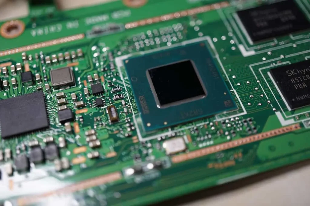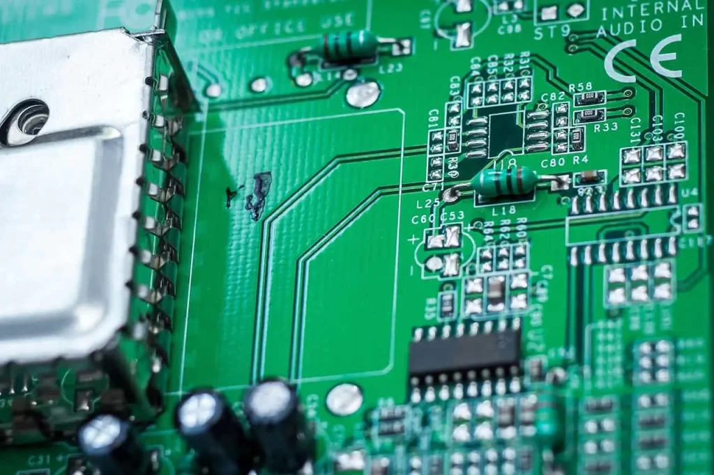

HDI PCB projects are not easy to judge from a quotation alone. A board may look simple in the Gerber files, but the real risk is often inside the structure. Microvias, fine lines, thin dielectric layers, stacked vias, and controlled impedance can all affect manufacturing yield and long-term reliability.
Many buyers compare HDI PCB suppliers by price first. That is understandable, but it can create risk. A low quotation does not help much if the supplier cannot review the stack-up, explain the microvia risk, or control the process before production starts.
A capable HDI PCB manufacturer should not only accept files and send back a price. The manufacturer should ask about layer structure, via type, impedance needs, material requirements, copper balance, surface finish, and inspection expectations. These questions show whether the supplier understands the real manufacturing work behind HDI PCB manufacturing.
Start with the HDI Build-Up Structure
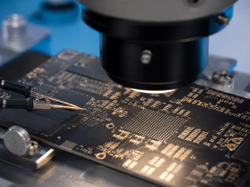
HDI build-up structure is one of the first items to review. A simple HDI PCB may use one microvia build-up layer. A more complex design may include blind vias, buried vias, stacked microvias, staggered microvias, and sequential lamination. Each structure creates a different level of manufacturing risk.
Buyers should not assume that every PCB factory can build every HDI structure. Some manufacturers may handle simple blind vias but may not have stable process control for more complex structures. The structure should be reviewed before quotation, not after the order has already moved forward.
The manufacturer should be able to explain whether the requested structure fits a stable production process. If the supplier only answers “yes” without checking the stack-up, via type, and lamination plan, that is a warning sign.
| HDI Structure Area | What Buyers Should Check |
|---|---|
| Microvia type | Confirm whether the design uses blind, buried, stacked, or staggered vias |
| Lamination plan | Check whether sequential lamination is required |
| Layer transition | Review how signals move between HDI layers |
| Copper balance | Check whether the stack-up may create warpage or plating risk |
| Impedance layers | Confirm which layers need impedance review |
This first review helps buyers avoid hidden process mismatches. It also helps the supplier confirm whether the design is ready for production or needs engineering adjustment.
Check Microvia Process Control
Microvia quality is central to HDI PCB reliability. Microvias are small, but they carry important electrical connections between layers. Poor laser drilling, weak plating, poor via filling, or poor pad registration can create failures that are hard to find from outside the board.
A manufacturer should understand how microvia design affects production risk. Via depth, pad size, dielectric thickness, copper plating, and layer alignment all matter. These details should be checked during DFM review before production release.
Buyers do not need to ask for every internal process setting. But they should ask how the manufacturer reviews microvia reliability. A serious supplier should be able to explain the main risk points and the inspection methods used for the project type.
Common microvia risks include:
These issues are not only manufacturing problems. They may also come from layout, stack-up design, material choice, or unclear fabrication notes. That is why early engineering review is important.
Review Fine Line and Registration Control
Fine line routing is common in HDI PCB designs. It helps route dense circuits under BGA packages, compact modules, and small electronic products. But smaller features also reduce process margin.
Buyers should confirm the manufacturer’s stable production limits before release. Exact line width, spacing, and registration capability should not be guessed. They must be confirmed from the project files and reviewed during DFM.
Registration control is also important. HDI boards often combine fine traces, microvias, buried vias, and multiple lamination cycles. Small alignment errors can affect annular ring, via capture, impedance, and production yield.
| Evaluation Point | Why It Matters | Buyer Check |
| Fine line routing | Affects etching yield and spacing risk | Confirm stable limits during DFM review |
| Microvia pad registration | Affects via connection reliability | Check pad size and layer alignment |
| BGA escape routing | Affects routing density and assembly risk | Review fanout and via placement |
| Copper distribution | Affects plating and lamination balance | Check copper balance across layers |
| Impedance traces | Affects signal quality | Confirm stack-up and trace geometry |
This table should be used as a review checklist, not as a fixed capability claim. Actual values must be confirmed based on the design and the manufacturer’s verified production process.
Evaluate Stack-Up and Material Support
Stack-up review is critical for HDI PCB projects. The stack-up controls impedance, lamination structure, dielectric thickness, copper balance, and via reliability. If it is not reviewed early, the design may need changes after quotation.
The manufacturer should be able to review the proposed layer structure and identify practical concerns. These concerns may include thin dielectric layers, copper imbalance, via stacking risk, impedance control, material selection, and surface finish compatibility.
Material support also matters. HDI PCBs may use standard FR4, high-Tg material, low-loss material, or other laminates depending on the application. Buyers should not select material only by name. They should confirm whether the material supports the electrical, thermal, and mechanical needs of the project.
When the design involves high-speed signals, compact routing, or controlled impedance, stack-up review should connect with PCB design review. A small routing or stack-up adjustment may reduce manufacturing risk before production starts.
Confirm Controlled Impedance Review
Controlled impedance is often required in HDI designs used for communication modules, high-speed electronics, and compact digital products. The manufacturer should review impedance requirements together with stack-up, trace width, spacing, copper thickness, and material data.
A supplier should not treat impedance as only a note in the Gerber file. Impedance depends on real stack-up construction and production tolerance. The buyer and manufacturer should agree on which traces need control and how the requirement will be checked.
Buyers should also confirm whether impedance testing or test coupons are needed. The exact method depends on the project requirement and customer standard. It should be reviewed before production release.
For HDI projects, impedance control is not separate from manufacturing. It connects directly with material selection, copper thickness, lamination control, and routing geometry.
Check Inspection and Reliability Methods
Inspection methods show how the manufacturer controls hidden risk. Standard visual inspection is not enough for many HDI PCB structures. Some defects are inside the board or under fine-pitch components after assembly.
For bare HDI PCB manufacturing, important inspection points may include electrical testing, microsection review, via quality checks, impedance testing, and material verification. If assembly is involved, AOI inspection and X-ray inspection may also be needed, especially for BGA and QFN packages.
Buyers should ask which inspection steps fit the design. The answer should depend on board structure, application risk, component type, and testing requirements. A fixed inspection answer for every project is not enough.
| Inspection Area | Purpose | When It Matters |
| Electrical testing | Checks open and short circuits | Needed for bare PCB verification |
| Microsection review | Checks plating and via structure | Useful for HDI and microvia reliability |
| Impedance testing | Verifies controlled impedance traces | Needed for high-speed signal layers |
| AOI inspection | Checks visible assembly defects | Useful after SMT assembly |
| X-ray inspection | Checks hidden solder joints | Important for BGA and QFN packages |
The right inspection plan depends on the product risk. A high-density board with fine-pitch parts usually needs more review than a simple low-density PCB.
Look at Engineering Review Before Quotation
Engineering review is one of the best ways to judge an HDI PCB manufacturer. A serious manufacturer should review the files before giving a final production answer. This review should include Gerber files, drill data, stack-up, material notes, impedance requirements, and special instructions.
A weak review often creates repeated questions later. It can also lead to quotation changes, production holds, or design changes after the buyer has already planned the project. These problems can create avoidable delays and extra communication.
The review should identify unclear files, missing notes, risky via structures, tight spacing areas, and material concerns. It should also explain what needs to be confirmed before production.
Buyers should prepare these files before asking for a serious quotation:
Complete files help the manufacturer review risk more clearly. They also help buyers compare quotations with fewer hidden differences.
Compare Prototype and Production Readiness
Prototype success does not always prove production readiness. A small prototype batch may pass inspection, but larger production can expose process margin issues. HDI PCB buyers should check whether the manufacturer can support both early samples and later production planning.
The main question is not only whether the manufacturer can build the first boards. The question is whether the process is stable enough for repeated production. This includes stack-up control, material consistency, plating control, registration control, inspection discipline, and engineering feedback.
Buyers should also check how the supplier handles design updates after prototype testing. If a prototype reveals routing, impedance, or assembly concerns, the supplier should help identify the cause and support a practical revision.
Production readiness is especially important for industrial, communication, medical, and server-related products. These applications often need stable process control and clear documentation before production release.
Watch for Supplier Warning Signs
Supplier warning signs are often visible before production starts. Buyers should pay attention to how the manufacturer answers technical questions. A low price is not helpful if the supplier cannot explain the process risk.
One warning sign is a quotation without technical questions. HDI projects usually need file review. If the manufacturer does not ask about stack-up, microvias, impedance, material, or inspection, the review may not be deep enough.
Another warning sign is overpromising. A supplier should not confirm every structure without checking the design. HDI manufacturing has real process limits, and those limits must be reviewed before production.
| Warning Sign | Possible Risk |
| No questions before quotation | Files may not have been reviewed carefully |
| Vague answers about microvias | Hidden via reliability may be overlooked |
| No stack-up discussion | Lamination and impedance risk may remain unclear |
| No inspection plan | Defects may be found too late |
| Overpromised capability | Actual process limits may not match the design |
A good manufacturer gives clear and practical answers. The supplier should explain what is possible, what needs review, and what may create production risk.
What Buyers Should Confirm Before Choosing a Supplier
Buyer confirmation should focus on process control, not only company introduction. The buyer should ask questions that reveal how the manufacturer handles HDI risk.
Useful questions include whether the supplier can review the stack-up, how microvia reliability is checked, which inspection methods are recommended, and what files are needed for a complete quotation. These questions help buyers compare suppliers more fairly.
Buyers should also confirm communication quality. HDI projects often need engineering feedback before production. If the supplier cannot explain issues clearly, small design questions may become larger production problems.
A practical supplier should help the buyer understand the risk before production starts. That is more useful than a simple “yes, we can make it” answer.
Planning Your HDI PCB Project
Evaluating an HDI PCB manufacturer should focus on real process control. Microvia quality, stack-up review, fine line control, material selection, impedance review, and inspection methods all affect the final board.
Before choosing a supplier, check whether the manufacturer can review your design and explain the risks clearly. This helps you compare quotations based on manufacturing readiness, not only price.
For engineering review and quotation support, please send your Gerber files, stack-up notes, and project requirements to sales@toplinecircuit.com.