


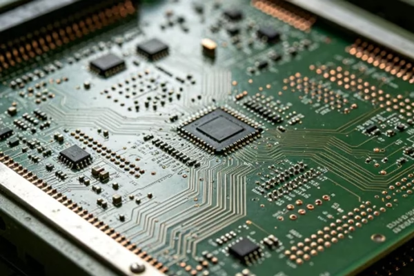
As modern military electronic equipment continues to evolve toward higher frequency, miniaturization, greater reliability, and complex integration, PCBs are no longer just platforms for carrying electronic components. They have become critical cores that directly affect weapon system stability, communication quality, radar performance, and data processing capability.Whether in military communication equipment, radar systems, navigation and control modules, unmanned aerial vehicle (UAV) platforms, or aerospace electronic systems, high-reliability PCB application solutions are essential. Compared with standard industrial PCBs, military and defense applications place greater emphasis on extreme environmental adaptability, including resistance to high and low temperatures, vibration, shock, humidity, electromagnetic interference, and the ability to operate stably over long periods.Therefore, a mature military PCB application solution typically requires systematic control from design, manufacturing, assembly, testing, to material selection. Military-grade PCBs are not only expected to “function,” but to “operate reliably over the long term.” Especially in complex battlefield environments, even minor failures may affect the operation of the entire system.
What is a PCB Application Solution for Military and Defense Industries?
A military PCB application solution refers to a complete set of high-reliability PCB design, manufacturing, assembly, and validation services developed specifically for military and defense electronic equipment.The biggest difference between military PCBs and ordinary consumer electronics PCBs lies in their “environmental adaptability” and “long-term stability.”
Military electronic equipment often operates under extreme conditions, such as:
- High-altitude low-temperature environments
- Desert high-temperature environments
- Marine high-humidity and high-salinity environments
- High-vibration and shock environments
- Strong electromagnetic interference environments
Therefore, PCB solutions must consider reliability from the initial design stage instead of attempting to solve issues after product completion.
Common Military PCB Application Areas
Military Communication Systems
Used in tactical communication, radio systems, encrypted communication devices, and similar applications requiring extremely high signal integrity and anti-interference capability.
Radar and RF Systems
High-frequency and high-speed signal transmission requires high-frequency substrates, impedance control, and low-loss structures.
Aerospace Electronics
Including flight control systems, navigation systems, and satellite electronic modules, all of which require strict control over weight, stability, and environmental resistance.
UAVs and Intelligent Equipment
These applications emphasize lightweight construction, miniaturization, and high integration while requiring vibration resistance and long-term operational stability.
Differences Between Military PCBs and Standard PCBs
| Comparison Item | Standard PCB | Military PCB |
| Operating Environment | Standard environments | Extreme and complex environments |
| Reliability Requirement | General | Extremely high |
| Service Life | Standard lifecycle | Long-term stable operation |
| Testing Standards | Standard electronics standards | Stricter military standards |
| Material Requirements | Standard materials | High heat resistance and high stability materials |
Important Considerations for Military-Grade PCB Design
Rigid PCB substrate: GF epoxy resin, flame-retardant, E-glass woven layers
Maximum panel size: 18 inches × 24 inches
Maximum layer count: 20 layers
Maximum board thickness: 100 mil
Minimum hole size:
Laser-drilled plated hole before plating: 0.007 inches (7 mil)
Through-hole drill size before plating: 0.01 inches (10 mil)
Aspect ratio:
Microvia: 0.75:1
Through-hole: 10:1
Minimum trace width/spacing: 0.004” / 0.004”
Surface finishes: HASL and ENIG
IPC Standards
Class 3 is the highest IPC standard. Military-grade PCB design and manufacturing should comply with standards applicable to IPC Class 3 PCBs. These standards include laminate selection, plating thickness, material certification, manufacturing processes, and inspection requirements.
How to Develop a Military PCB Application Solution
The implementation process for military PCB solutions is generally more complex than for ordinary electronic products because military projects must satisfy not only functional requirements but also long-term reliability, production consistency, and maintainability.
The process typically includes:
Requirement Analysis Stage
This stage confirms:Product operating environment、Frequency range、Operating temperature、Structural limitations、Reliability level.
For example:Is high-temperature resistance required?Are high-frequency signals involved?Will the system run continuously for long periods?Is vibration resistance required?Will the device operate in strong electromagnetic environments?
Only after clarifying these requirements can subsequent designs truly meet military standards.
PCB Structural Design Stage
Military PCBs commonly use:
- Multilayer structures
- HDI high-density designs
- Rigid-flex structures
- High-frequency/high-speed routing structures
Design considerations include:
- Impedance control
- Power integrity
- Ground plane design
- Thermal management paths
EMC design:This stage determines whether the PCB can operate stably in the future.
Manufacturing and Assembly Stage
Military PCB manufacturing places much greater emphasis on consistency control than ordinary PCB production.
Key focuses include:
- Via copper reliability
- Lamination stability
- Soldering quality
- AOI inspection
- X-ray inspection
- Cleanliness control
During SMT assembly, additional controls include:
- Reflow temperature profiles
- Component alignment
- Void ratio control
- Solder joint fatigue risk management
Key Manufacturing Focus Areas
| Manufacturing Stage | Key Control Focus |
| Lamination | Prevent delamination and deformation |
| Drilling | Improve hole wall reliability |
| Plating | Ensure sufficient copper thickness |
| Soldering | Improve solder joint lifespan |
| Inspection | Detect potential defects early |
Reliability Validation Stage
This is one of the most critical stages for military PCBs.Common tests include:High and low temperature cycling tests;Humidity and heat tests;Vibration tests;Shock tests;Salt spray tests;Aging tests;EMI/EMC tests.These tests help identify hidden risks in advance and improve overall system reliability.
How to Improve Military PCB Application Solutions
The real challenge of military PCBs is not simply “making them work,” but ensuring “long-term stable operation.”Many PCBs may function correctly in laboratory conditions but encounter issues in complex environments, such as:
- Solder joint cracking and delamination
- Signal distortion
- High-frequency losses
- Thermal failures
- Electromagnetic interference
Therefore, technical detail control is extremely important.
High-Frequency and High-Speed Design
Modern military equipment extensively uses radar, RF communication, and high-speed data systems.As a result, PCBs must carefully control:Impedance continuity;Return paths;CrOsstalk;Signal loss.Especially in high-frequency applications, routing length, corner design, and stack-up structures significantly affect signal quality.
Thermal Management Design
Military equipment often operates continuously.
Poor heat dissipation may result in:
- Increased chip temperatures
- Reduced performance
- Shortened service life
Therefore, PCBs should:
- Increase thermal copper layers
- Optimize thermal vias
- Design heat spreading structures
- Properly arrange power components
Vibration Resistance Design
Military equipment frequently experiences:Flight vibration;Vehicle vibration;Launch shock.Therefore, PCB mechanical stability must be enhanced.
Common methods include:dding mounting holes;Reinforcing frame structures;Using rigid-flex boards.Optimizing weight distribution of large components.
Electromagnetic Compatibility (EMC) Design
Complex military systems often involve multiple devices operating simultaneously.Insufficient anti-interference capability may lead to:Data errors、Communication abnormalities、Radar misjudgment.Therefore, it is necessary to optimize:Grounding structures\Shielding design\Power filtering\Partitioned layout.
Technical Optimization Directions
| Technical Area | Optimization Goal |
| High-frequency design | Improve signal stability |
| Thermal management | Reduce component temperature rise |
| Mechanical structure | Improve vibration resistance |
| EMC design | Reduce electromagnetic interference |
What Materials Are Used in Military PCB Solutions?
Military PCBs require extremely high material standards because materials directly affect:
- Heat resistance
- High-frequency performance
- Mechanical strength
- Long-term stability
High-Frequency Materials
Used in radar and RF systems.
Requirements:
- Low dielectric loss
- Stable dielectric constant
- Stable high-frequency signal performance
High-TG Materials
Suitable for high-temperature environments.
Characteristics:
- Better thermal stability
- Lower risk of delamination
- Better suited for long-term operation
Rigid-Flex Materials
Suitable for:
- Aerospace electronics
- UAVs
- Space-constrained equipment
Advantages:
- Reduced connectors
- Lower weight
- Improved reliability
High-Reliability Surface Finishes
Common military PCB surface finishes include:
- ENIG
- Immersion silver
- Immersion tin
Main purposes:
- Improve solderability
- Reduce oxidation risk
- Enhance long-term stability
Common Material Categories
| Material Type | Application Area | Core Advantage |
| High-frequency materials | Radar / communication | Low loss |
| High-TG materials | High-temperature equipment | Strong thermal stability |
| Flexible materials | Aerospace electronics | Bendable |
| Rigid-flex materials | Compact devices | High integration |
Why Do Military PCBs Emphasize “One-Stop Solutions”?
Many customers find that military PCB projects usually have long development cycles and often require repeated modifications due to mismatches between design, manufacturing, and assembly.If design firms, PCB manufacturers, and SMT factories communicate independently, issues may arise such as:
- Misinterpretation of documents
- Process incompatibility
- Inconsistent testing standards
- Project delays
The advantage of a one-stop PCB solution is that:
- Manufacturing processes are considered during the design stage
- Assembly requirements are considered during manufacturing
- Test feedback is used to optimize design structures
This not only reduces rework but also improves project efficiency, especially for high-reliability military and defense projects.
Conclusion
The importance of PCB application solutions in military and defense industries is no longer limited to “electrical connectivity.” It directly impacts the stability, safety, and long-term reliability of the entire system.As modern military electronics continue evolving toward high speed, high frequency, and intelligent systems, PCBs are taking on increasingly important roles.
From initial design and structural planning to manufacturing processes, assembly testing, material selection, and reliability validation, every stage affects final product quality.For military projects, a truly reliable PCB solution is not just about producing the product, but ensuring that it can operate stably for the long term in complex environments.
Your Trusted One-Stop PCB Manufacturing and Assembly Partner
Founded in 2000 and headquartered in Shenzhen, China, Toplay Circuit is an electronic solutions provider offering PCB layout, manufacturing, assembly, testing, and validation services. Its products include highly reliable flexible PCBs, rigid-flex boards, RF/microwave boards, HDI boards, and rigid PCBs.As a recognized technology leader, Toplay Circuit provides genuinely fast turnaround times, with all solutions completed in-house to create a true one-stop service experience.
We provide one-stop PCB manufacturing and assembly services covering prototyping, mass production, SMT/DIP assembly, testing, and delivery. From engineering review to shipment, we focus on quality control and delivery reliability. Clear communication helps customers transition from prototype to production more efficiently.