PCB prototyping is a crucial step in transforming design drawings into physical circuit boards, and a key step in verifying the correctness and manufacturability of the design. By standardizing the process and conducting thorough checks, production risks can be effectively reduced and finished product quality improved. Understanding the complete process and key points helps improve prototyping efficiency and success rate.
Design Document Preparation Before PCB Prototyping
Before entering the prototyping stage, complete and standardized design documents need to be prepared. Common documents include Gerber files, drilling files, and assembly drawings, which guide the manufacturing plant in processing. When exporting files, it should be confirmed that the information of each layer is complete, including circuit layers, solder mask layers, and silkscreen layers. Naming rules should be clear and consistent to avoid identification errors during production. Checking the file content in advance can reduce communication costs and improve prototyping efficiency.
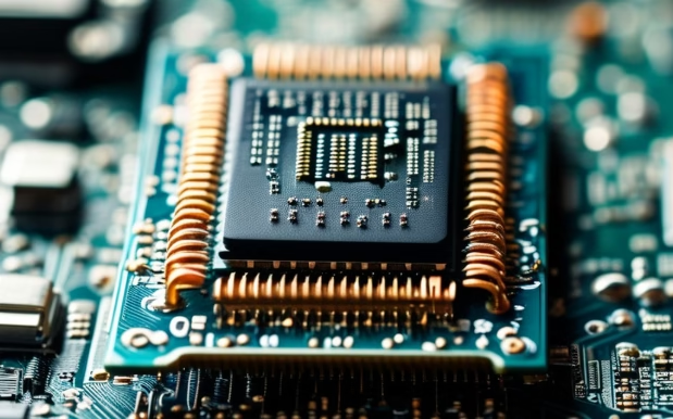
Prototyping Process and Production Steps
PCB prototyping usually follows a fixed process, requiring the cooperation of multiple stages from design confirmation to finished product output.
- Design Document Review: The manufacturing plant checks the documents to confirm whether they meet the processing requirements.
- Engineering Processing: Optimize and adjust the circuitry to ensure it meets manufacturing process standards.
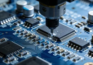
- Board Making and Exposure: Transfer the circuit pattern to the board to form a preliminary structure.
- Etching and Drilling: Remove excess copper and complete hole machining.
- Surface Treatment and Inspection: Perform tin plating or immersion gold treatment and check electrical performance.
Each step affects the final quality and requires strict control.
Key Points for Material and Process Selection
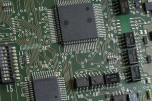
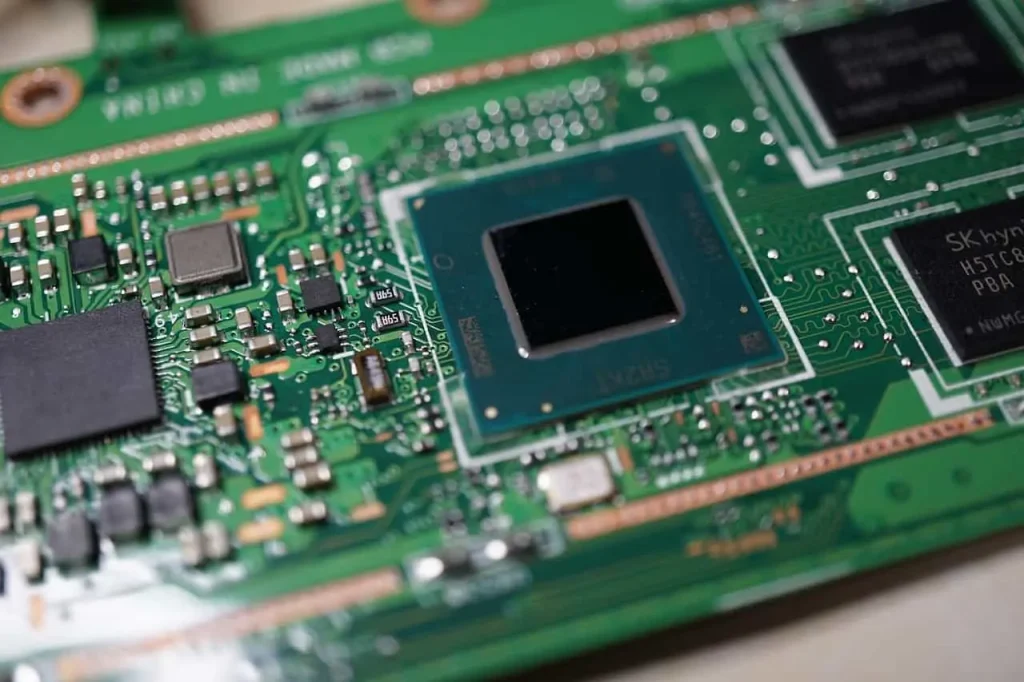
During prototyping, the selection of materials and processes directly affects the performance of the finished product. FR-4 is a commonly used substrate, suitable for most electronic products; for high-frequency applications, higher performance materials can be selected. Surface treatment methods include tin plating, immersion gold, and OSP, etc., with different processes exhibiting different performance in solderability and durability. Selecting appropriate materials and processes according to actual needs can improve the reliability of the circuit board.
Common Problems and Prevention Methods
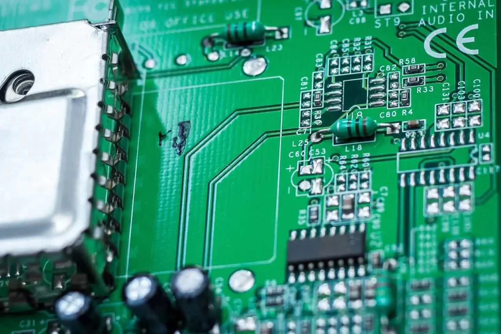
During PCB prototyping, some problems are prone to occur, such as broken circuits, misaligned holes, or unreasonable pad design. During the design phase, ensure that the trace spacing meets specifications to avoid short-circuit risks. Hole diameter design must match component pins to ensure soldering quality. For high-density designs, special attention should be paid to line width and spacing control. Early inspection and optimization can reduce the probability of rework.
Post-Prototyping Inspection and Optimization Recommendations
After prototyping, functional testing and visual inspection of the circuit board are necessary. Power-on testing can confirm whether the circuit is operating normally, and at the same time, check for defects in the pads and traces. Based on the test results, make necessary adjustments to the design to prepare for subsequent mass production. Continuous optimization of design details can improve product stability and consistency.
PCB prototyping is a crucial bridge connecting design and production. Standardized processes and rigorous inspections ensure stable circuit board quality. Mastering the prototyping process and key considerations helps improve development efficiency and allows products to enter the practical application stage more quickly.