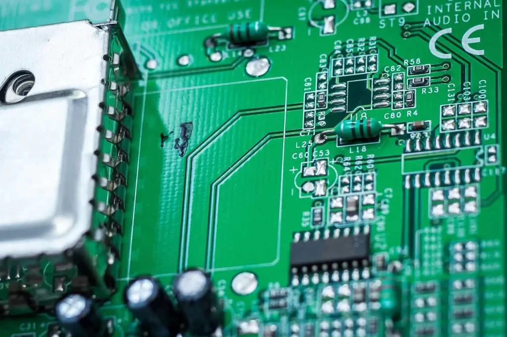
PCB (Printed Circuit Board) manufacturing is a multi-step, high-precision industrial process that transforms circuit designs into usable electronic devices. From initial design data to final board delivery, every step requires strict control to ensure the electrical performance and mechanical stability of the circuit. As electronic products continue to evolve towards miniaturization and high performance, PCB manufacturing processes have become more complex, placing higher demands on equipment precision, material properties, and process flows.
The PCB manufacturing process includes several key steps such as design output, material preparation, pattern transfer, etching, electroplating, lamination, surface treatment, and testing. Each step is interconnected, and a problem in any step can affect the final product quality. Therefore, choosing a manufacturer with complete manufacturing capabilities is crucial. For example, Topray Circuits integrates PCB layout, manufacturing, assembly, and testing resources to provide a one-stop service, improving production efficiency and effectively ensuring product consistency and reliability.
Core Steps in PCB Manufacturing
· Engineering Design and Data Processing
Based on the Gerber files provided by the customer, process evaluation is conducted to optimize production parameters.
• Substrate Preparation and Cutting
Select suitable copper-clad laminate (CCL) material and cut it to the required dimensions for production.
• Inner Layer Circuit Fabrication
Transfer the circuit pattern onto the copper layer through exposure and development, followed by etching to form the circuitry.
• Lamination (Multilayer Board)
Bond multiple layers of circuit boards together under high temperature and pressure to form a unified structure.
• Drilling
Use mechanical or laser drilling to provide pathways for components and interlayer connections.
• Electroplating and Hole Metallization
Deposit metal on the hole walls to achieve electrical connections between the circuit layers.
• Outer Layer Circuit Fabrication
Repeat the pattern transfer and etching process to form the outer layer circuitry of the PCB.
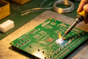
• Surface Treatment
Perform treatments such as tin plating and immersion gold plating to improve solderability and oxidation resistance.
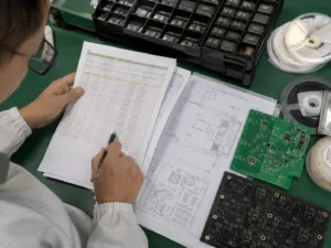
• Forming and Inspection
Complete the final product through cutting, testing, and other steps, and conduct quality inspection.
Analysis of Different PCB Manufacturing Methods
In PCB manufacturing, different product types correspond to different process methods. For example, the manufacturing process for single-sided boards is relatively simple, requiring only one circuit fabrication; while multilayer boards require multiple laminations and alignment controls, significantly increasing process complexity. HDI PCBs differ significantly from traditional PCBs in drilling and electroplating. HDI requires laser drilling and micro-hole electroplating technology, placing higher demands on equipment and processes. Flexible PCBs, on the other hand, differ in materials and processing methods, requiring attention to the stability of the flexible substrate. Furthermore, in terms of surface treatment, conventional tin plating is less expensive, but immersion gold is more popular in high-end products due to its superior reliability and solderability. Therefore, there is no absolute superiority or inferiority among different manufacturing methods; the choice depends on product requirements.
Frequently Asked Questions
Q: Why is the PCB manufacturing process so complex?
A: Because each layer of circuitry and connection requires precise control to ensure stable electrical performance.
Q: What is the purpose of electroplating?
A: It is used to deposit metal on the hole walls, enabling conductivity between different layers.
Q: What is the significance of surface treatment?
A: It prevents oxidation and improves soldering quality.
Q: Why are multilayer PCBs more expensive?
A: Because they involve more processing steps, require higher precision, and are more difficult to manufacture.
Different industries have different requirements for PCB technology
For example, in consumer electronics products, such as smartphone motherboards, multilayer PCBs or even HDI structures are commonly used. These products require multiple laminations and precision machining to achieve high-density wiring. In industrial equipment, the manufacturing process for rigid PCBs is relatively stable, but electroplating and testing still require strict control to ensure long-term reliable operation. In high-end communication equipment, the manufacturing of RF PCBs is even more complex, with extremely high requirements for materials and processes. In these cases, specialized manufacturers like Topray Circuits can provide complete solutions from design to testing, tailored to different application needs, ensuring product performance meets expectations.
From inner layer circuit fabrication to final surface treatment, every step of the PCB manufacturing process must be strictly performed according to standards. For example, exposure accuracy determines circuit quality, electroplating uniformity affects conductivity, and lamination processes relate to overall structural stability. Only by closely integrating design, manufacturing, and testing can defect rates be effectively reduced and product consistency improved. By leveraging the capabilities of one-stop shops like Topray Circuits, efficient collaboration can be achieved throughout the entire process, ensuring comprehensive quality control from source to finished product.Overall, PCB manufacturing is not just a standardized process, but a systematic engineering project. Only by achieving standardization and precision in every detail can we ensure that the final product possesses excellent performance and reliability, thereby meeting the needs of diverse electronic applications.